6502.org Forum  Projects  Code  Documents  Tools  Forum
It is currently Mon Apr 29, 2024 1:43 am

All times are UTC


Post new topic Reply to topic  [ 8 posts ] 
Author Message
PostPosted: Fri Jan 09, 2015 12:04 am 
Online
User avatar

Joined: Fri Dec 11, 2009 3:50 pm
Posts: 3349
Location: Ontario, Canada
A discussion elsewhere about memory-expansion hardware prompted me inform or remind forum readers about the 74_670 dual-port 4x4 register-file. Available in LS, HC and (at one time) AC processes, this 16-pin IC is a powerful addition to the (discrete-)hardware hacker's toolkit. Uses include:

  • MMU and memory-mapping schemes, of course.
  • acting as a mailbox to link one processor with another
  • linking a processor with a writable lookup table whose read section is connected in the role of a priority encoder, chip-select decoder, or any similar translation whose behavior you might wish to update on the fly.

FWIW, a less obvious (and less common) application is when you simply need a 4-bit transparent latch, but a '573/whatever won't do because you want some extra enable inputs. To accomplish this, just re-designate the 670's write address inputs as active-high and/or active-low write enables. Hardwire the read address to match the high/low decisions you made. Only that one RAM location will ever get read. The remaining three locations constitute write-only memory! :D

-- Jeff

ps- 'hc670s are plentiful but 'ac670s are hard to find. I know of only one supplier who claims to have stock.
Attachment:
74ac670.pdf [60.98 KiB]
Downloaded 139 times
Attachment:
74HC_HCT670_CNV.pdf [77.58 KiB]
Downloaded 123 times
Attachment:
670 symbol.gif
670 symbol.gif [ 9.89 KiB | Viewed 2106 times ]
Attachment:
File comment: this circuit is like a '670 (except the 573's make it 8 bits wide instead of 4)
'670 logic equivalent.png
'670 logic equivalent.png [ 7.53 KiB | Viewed 1419 times ]

_________________
In 1988 my 65C02 got six new registers and 44 new full-speed instructions!
https://laughtonelectronics.com/Arcana/ ... mmary.html


Last edited by Dr Jefyll on Sun Mar 18, 2018 10:29 pm, edited 2 times in total.

Top
 Profile  
Reply with quote  
PostPosted: Fri Jan 09, 2015 1:41 pm 
Offline
User avatar

Joined: Mon Dec 08, 2008 6:32 pm
Posts: 143
Location: Brighton, England
A useful device, I used it as a 4 to 16 colour palette device on a very old video interface.

The only thing to watch out for is that, as Dr Jefyll says, if the read address and the write address are the same, the device becomes transparent. This may cause invalid data to appear at the outputs when writing to the device, this is virtually certain to happen if the WE strobe goes low before the data bus has settled.

_________________
Shift to the left,
Shift to the right,
Mask in, Mask Out,
BYTE! BYTE! BYTE!


Top
 Profile  
Reply with quote  
PostPosted: Tue Jan 13, 2015 11:37 pm 
Offline
User avatar

Joined: Thu Jun 23, 2011 2:12 am
Posts: 229
Location: Rancho Cucamonga, California
A regular SRAM chip (non dual-channel) should be quite fast enough nowadays to work as a memory manager. I've been thinking of this idea for a while for a possible future project with a 65C02 and a large amount of RAM.

Let's say you have a big SRAM chip, say or 16 megabytes or so. That would use 24 address lines but the 65C02 only has 16 address lines.

So you use an extra (8 bit wide) RAM chip to generate the 8 extra address lines from a secondary RAM (the secondary RAM data bus lines would be the primary RAM's top 8 address lines). It doesn't have to be big. For example if you would have a 256 byte SRAM chip as secondary RAM, you could divide your 64K addresses into 256 areas, each of which can be mapped into a different area of the 16MB main RAM. Of course you would also need to map the secondary RAM into memory so you can change it, so the glue logic may be a bit of a challenge, but it sure is possible and probably not too hard.

===Jac


Top
 Profile  
Reply with quote  
PostPosted: Wed Jan 14, 2015 1:42 am 
Online
User avatar

Joined: Fri Dec 11, 2009 3:50 pm
Posts: 3349
Location: Ontario, Canada
jac_goudsmit wrote:
the secondary RAM data bus lines would be the primary RAM's top 8 address lines
Hi Jac -- This sounds like what Druzyek suggested in the discussion I linked to from the lead post. The latest consensus is it won't work unless a latch is included -- but maybe that's what you meant. Anyway, in this thread I thought we could focus on the '670. The facts it's just a 16-pin -- and dual-port -- make for many applications, not just MMUs.

PaulF wrote:
I used it as a 4 to 16 colour palette device on a very old video interface.
Thanks for checking in, Paul. Come to think of it, I did that too (but momentarily forgot). :oops: "Great minds think alike" aka "fools never differ" !!

PaulF wrote:
if the read address and the write address are the same, the device becomes transparent. This may cause invalid data to appear at the outputs when writing to the device, this is virtually certain to happen if the WE strobe goes low before the data bus has settled.
You're right, that needs to be highlighted. Of course waiting for the inputs to settle is SOP, especially with transparent (as opposed to edge-triggered) storage.

-- Jeff

_________________
In 1988 my 65C02 got six new registers and 44 new full-speed instructions!
https://laughtonelectronics.com/Arcana/ ... mmary.html


Top
 Profile  
Reply with quote  
PostPosted: Sun Oct 15, 2017 4:22 am 
Offline
User avatar

Joined: Wed Feb 13, 2013 1:38 pm
Posts: 586
Location: Michigan, USA
I haven't quite figured out how you might use the '670 for bank switching. Are there any examples I could study?

TIA... Cheerful regards, Mike


Top
 Profile  
Reply with quote  
PostPosted: Sun Oct 15, 2017 5:01 am 
Offline
User avatar

Joined: Mon May 12, 2014 6:18 pm
Posts: 365
Quote:
I haven't quite figured out how you might use the '670 for bank switching.
The way I was thinking was to just use it as a set of latches. If you had 512k of RAM, for example, let the 4 outputs drive A15-A18. That way you would have 4 different 32k windows into the RAM if you wanted. Like PaulF said, though, it will become transparent when you write to it, so I think you would need to run the code to set a new values from outside the RAM being bank switched.

Has anyone found the AC version? I was just looking today and didn't find one.


Top
 Profile  
Reply with quote  
PostPosted: Sun Oct 15, 2017 7:48 am 
Online
User avatar

Joined: Fri Dec 11, 2009 3:50 pm
Posts: 3349
Location: Ontario, Canada
Thanks for the suggestion -- examples would be good. :) Alarm Siren has a scheme that can illustrate use of a '670, so I've taken the liberty of reproducing and altering his diagram.

Attachment:
Logic (rev.).png
Logic (rev.).png [ 14.96 KiB | Viewed 1730 times ]

At the bottom there's a VIA acting as a 3-bit Bank Register. And it's easy to imagine a 74_573 transparent latch doing basically the same job (as shown in red). Essentially you write the desired Bank number from the data bus to the VIA (or to the '573), and thereafter the bank number gets read out on pins which hardware interprets as the upper address bits when the program accesses the "window" at 8000-BFFF. This is a time-tested approach; solid and familiar territory.

Unfortunately it can be a bottleneck having just one Bank Register. There's save/restore overhead if its use needs to be shared with an Interrupt Service Routine, and even simple non-interrupt tasks face challenges because having only one window means only one bank can be accessible at a time. For example, it's very awkward to compare strings or other data structures if each resides in a different bank. Also you can't copy directly from one extended Bank to another. Instead you're forced to copy from extended RAM to base RAM then (after altering the Bank Register) copy again to extended RAM in the destination Bank.

The '670 is really just four transparent latches in one package, and that's a big help in keeping the chip count low if you choose to implement two (or even four) Bank Registers to relieve the bottleneck. The '670 read select and write select inputs dictate which latch will be active, and there are different ways you might want to manage those inputs. One option is to simply give the 64K base map two "windows" into extended RAM. You'd decode the address to determine which window is being referenced, and thereby derive a signal to drive the aforementioned '670 read select input. Write select is somewhat similar but used when you're loading up the '670 registers prior to use. By writing to the '670 you can "aim" one window at one bank and the other window at another. Both windows become immediately accessible, and doing a copy or comparison suddenly becomes a great deal faster. HTH, and let me know please if there's anything important I missed.

Druzyek, I missed your post while typing my own. Nice to see we share that view of a 670 as basically a set of latches. :)

With my KK Computer I kind of went to town, 670-wise. :roll: It has four bank registers and they're 8 bits wide.

Also there's a drastically different mechanism to control when the 670's engage. A window scheme uses ordinary 6502 instructions, and the VIA/'573/'670 kicks in only for cycles during which an access within the designated window results -- that's how we get a cycle-accurate answer to the "when" question. Typically as the instruction concludes there's a transition to the other bank; finally, for one cycle only, there's a data access (read or write) of the other bank. That concludes the instruction and the access to the other bank. It's a fairly simple scheme to implement, but unfortunately the windows are smaller than you might wish because they and the base RAM must all fit within 64K. In fact the total of everything that's immediately accessible never exceeds 64K. In contrast, KK has new instructions, and external microcode that "knows" what the CPU is doing on every cycle. So again we get a cycle-accurate answer to the "when" question, but the cues comes from microcode, not an address decoder waiting for the window to get touched. The need for the window goes out the window! :P Now every bank can be a full 64K in size -- and as much as 256K can be made immediately accessible. That's assuming 4 Bank Registers, and you could increase that if your new instruction set can be adapted to accommodate. Another advantage of breaking the window is that 64K chunks are much faster to process than non-64K chunks when the goal is to simulate a "flat" aka linear 16 MB space. Flatness isn't a major concern when it comes to storing code, but if it's data which your new address space is going to be filled with then flat addressing is a boon, especially for hosting and examining objects bigger than 64K.

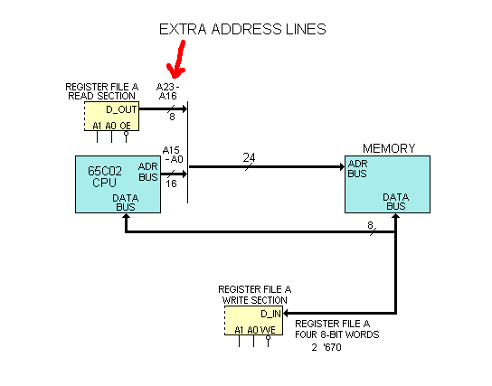
The KK Computer is summarized here, and the block diagram shows the 670's but to clarify here's an edited excerpt. The 670 is drawn in two pieces but it connects in much the same way as in the example above (accepting writes from the data bus and outputting high address bits).

-- Jeff
[multiple edits...]
Attachment:
KK_block_diagram_excerpt.png
KK_block_diagram_excerpt.png [ 5.5 KiB | Viewed 1730 times ]

_________________
In 1988 my 65C02 got six new registers and 44 new full-speed instructions!
https://laughtonelectronics.com/Arcana/ ... mmary.html


Top
 Profile  
Reply with quote  
PostPosted: Mon Oct 16, 2017 11:38 am 
Offline
User avatar

Joined: Wed Feb 13, 2013 1:38 pm
Posts: 586
Location: Michigan, USA
Ah! Light bulb moment. Thank you very much, Gentlemen.

Cheerful regards, Mike


Top
 Profile  
Reply with quote  
Display posts from previous:  Sort by  
Post new topic Reply to topic  [ 8 posts ] 

All times are UTC


Who is online

Users browsing this forum: Dr Jefyll and 37 guests


You cannot post new topics in this forum
You cannot reply to topics in this forum
You cannot edit your posts in this forum
You cannot delete your posts in this forum
You cannot post attachments in this forum

Search for:
Jump to: