6502.org Forum  Projects  Code  Documents  Tools  Forum
It is currently Thu Apr 25, 2024 10:13 am

All times are UTC


Post new topic Reply to topic  [ 37 posts ]  Go to page Previous  1, 2, 3  Next
Author Message
PostPosted: Sat Mar 01, 2014 10:58 am 
Offline
User avatar

Joined: Fri Dec 11, 2009 3:50 pm
Posts: 3346
Location: Ontario, Canada
Earlier in this thread...
GARTHWILSON wrote:
full address decoding [...] would reduce the maximum clock speed, unless I resorted to programmable logic.

One way to preserve maximum clock speed, even without programmable logic, is to wait-state the I/O. The resultant performance trade-off can be minimized, as explained later.

In the case of a 'C02 system that's lacking programmable logic, clocked at maximum speed, and using the wait-state solution, I/O in zero-page is still a clear win. An '816 system subject to all the same restrictions will have no benefit performance-wise; however, it and the 'C02 both save program memory by using zero-page/direct-page addressing mode.

Further improvement occurs if any of the restrictions are relaxed (slower clock, and/or programmable logic is available), because wait states become unnecessary. A 'C02 system will get 100% of the benefit of I/O in zero-page. Unfortunately the '816 doesn't have SMB RMB BBS and BBR instructions, but (like the 'C02) it will save one cycle and one byte for each occurrence of LDA STA BIT TSB TRB etc with zero-page/direct-page addressing.

Attachment:
zero-page decoder and wait-state generator.gif
zero-page decoder and wait-state generator.gif [ 18.04 KiB | Viewed 1165 times ]

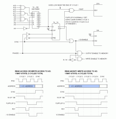
The circuit above includes wait state logic and full decoding for a 6522 VIA mapped into zero page. Read-Modify-Write instructions incur only one wait state, not three. This preserves the substantial performance advantage offered by SMB and RMB -- instructions custom tailored for fast I/O! The more general R-M-W instructions such as INC DEC TSB and TRB also incur only one wait state, as do simple reads and writes such as BIT LDA STA AND ORA etc.

If I were building this I'd use 74LVC1G332's for the three 3-input OR gates at the top left. These guys come in a painfully tiny 6-pin DIP but boast 3-ns maximum propagation delay. The 74_138 decoder is available in a long list of high-speed families, including 74AC and 74BCT.

In the timing diagrams, cycle one is the wait state, when the zero-page address first appears. Because no data is transfered in cycle 1, we're freed from the usual stipulation that the VIA CS must be asserted before Phase 2 begins. Instead it's sufficient merely to bring the CPU RDY input low tPCS before Phase 2 ends.

Memory is not yet inhibited, so an unused memory access occurs in cycle one. Since RDY gets pulled low in cycle 1, cycle 2 is the same address all over again -- but this time accessing the VIA instead of memory. In cycle 2 there's no difficulty getting the VIA chip-select asserted before Phase 2 begins, because tADS (the CPU address delay) and the decoder propagation delay have already elapsed -- those signals are stable.

Next we have either the beginning of the next instruction (marked by SYNC), or cycles 3 & 4 and then the beginning of the next instruction (marked by SYNC). :) It's actually the SYNC signal that ends the VIA chip-select -- and here again we avoid the decoder propagation delay. The SYNC signal is passed to the VIA with just a single gate-delay (the 2-input OR). It's always this same path that ends the VIA chip select, regardless of whether the access is read-modify-write or just a simple read or write. That's why the two timing diagrams end with the identical sequence.

-- Jeff

_________________
In 1988 my 65C02 got six new registers and 44 new full-speed instructions!
https://laughtonelectronics.com/Arcana/ ... mmary.html


Last edited by Dr Jefyll on Wed Jun 11, 2014 4:01 am, edited 1 time in total.

Top
 Profile  
Reply with quote  
PostPosted: Sat Mar 01, 2014 5:19 pm 
Offline
User avatar

Joined: Sun Jun 30, 2013 10:26 pm
Posts: 1925
Location: Sacramento, CA, USA
I am not personally qualified to comment on the feasibility of your design, but I somehow feel the need to congratulate you for such a well-polished and attractive post, doc!

Mike


Top
 Profile  
Reply with quote  
PostPosted: Sat Mar 01, 2014 7:57 pm 
Offline
User avatar

Joined: Fri Dec 11, 2009 3:50 pm
Posts: 3346
Location: Ontario, Canada
Thanks, Mike. I'm glad you find that post attractive, 'cause this one is gonna make ya wanna retch!
Attachment:
DBV IC package.gif
DBV IC package.gif [ 325.81 KiB | Viewed 1149 times ]
Did I mention that the 74LVC1G332 comes in a painfully tiny package? Actually you have three options to choose from: painfully tiny, agonizingly tiny, and just stupifyingly small. I'd recommend the comparatively gargantuan DBV package, shown here to scale on a .1" grid of plate-through holes. Some people would find these excessively small for proto-board hacking, but I'm too stubborn to admit defeat, so here's how I'd deal with these puppies. (Really you want a PCB for these if you can manage it.)

In the arrangement at the top left we have the benefit of soldering four pins to the board, with the remaining two pins (2 & 5) requiring flying leads. Unfortunately those two are the power supply, and deserve the best connections. The other arrangement uses four flying leads, but the power pins can have solid connections (and possibly a SMD bypass cap) directly on the opposite side. Putting a little bend in the other four pins will ensure they don't contact anything they shouldn't, and wirewrap wire is a workable gauge for the flying leads.

Needless to say, pairing some 74LVC1G332's with a '138 is just one of many ways to decode a zero-page address. But the 3ns prop delay makes 74LVC1G332's very attractive.

-- Jeff

_________________
In 1988 my 65C02 got six new registers and 44 new full-speed instructions!
https://laughtonelectronics.com/Arcana/ ... mmary.html


Top
 Profile  
Reply with quote  
PostPosted: Sun Mar 02, 2014 12:54 am 
Offline
User avatar

Joined: Sun Jun 30, 2013 10:26 pm
Posts: 1925
Location: Sacramento, CA, USA
How about one of these little guys, Jeff?

Attachment:
sot363.JPG
sot363.JPG [ 53.23 KiB | Viewed 1137 times ]


Mike


Top
 Profile  
Reply with quote  
PostPosted: Sun Mar 02, 2014 1:09 am 
Offline
User avatar

Joined: Fri Dec 11, 2009 3:50 pm
Posts: 3346
Location: Ontario, Canada
barrym95838 wrote:
How about one of these little guys, Jeff?
I've used stuff like that but it's rare to find one I like. For the 6-pin I admit it works out quite nicely, so that's good to mention -- thanks. I guess my reservations apply more to the larger adapters, which typically...
  • hog PCB space, and
  • make no special accommodation for the power supply traces

It has occurred to me to submit improved designs to a local manufacturer of these boards, or to just make my own. But in the meanwhile I usually just do without. And nothing'll beat the density of one of my Hacker Specials!

-- Jeff

_________________
In 1988 my 65C02 got six new registers and 44 new full-speed instructions!
https://laughtonelectronics.com/Arcana/ ... mmary.html


Top
 Profile  
Reply with quote  
PostPosted: Sun Mar 02, 2014 1:41 am 
Offline

Joined: Mon Mar 02, 2009 7:27 pm
Posts: 3258
Location: NC, USA
Am I missing something here? Or do you guys need some serious help?!
CPLD! FPGA!!

_________________
65Org16:https://github.com/ElEctric-EyE/verilog-6502


Top
 Profile  
Reply with quote  
PostPosted: Sun Mar 02, 2014 2:01 am 
Offline
User avatar

Joined: Fri Dec 11, 2009 3:50 pm
Posts: 3346
Location: Ontario, Canada
I don't mind being teased, Sam. :D There's a certain fascination with these hard-wiring challenges, and it can get perverse. But if you look back about a dozen posts you'll see the drift is programmable-logic alternatives.

BTW I've been using programmable logic since about 1980. A bipolar PROM can really make a lot of jelly-bean logic go away.

_________________
In 1988 my 65C02 got six new registers and 44 new full-speed instructions!
https://laughtonelectronics.com/Arcana/ ... mmary.html


Top
 Profile  
Reply with quote  
PostPosted: Sun Mar 02, 2014 2:40 am 
Offline
User avatar

Joined: Sun Jun 30, 2013 10:26 pm
Posts: 1925
Location: Sacramento, CA, USA
ElEctric_EyE wrote:
Am I missing something here? Or do you guys need some serious help?!
CPLD! FPGA!!

Chillax, bro! 8) We're not trying to build a daily driver here, just tinkering around with a pile of nuts and bolts, trying to sculpt something retro-cool. I'm here to learn and be entertained, not to change the world. :D

Mike


Top
 Profile  
Reply with quote  
PostPosted: Sun Mar 02, 2014 6:37 am 
Offline
User avatar

Joined: Thu May 28, 2009 9:46 pm
Posts: 8142
Location: Midwestern USA
Dr Jefyll wrote:
A bipolar PROM can really make a lot of jelly-bean logic go away.

Yep, poor man's PLA. :D The prototype of the Lt. Kernal hard drive subsystem used an EPROM in the host adapter for glue logic. Not real speedy but it did work.

_________________
x86?  We ain't got no x86.  We don't NEED no stinking x86!


Top
 Profile  
Reply with quote  
PostPosted: Tue Jul 01, 2014 9:15 pm 
Offline
User avatar

Joined: Sun Dec 29, 2002 8:56 pm
Posts: 449
Location: Canada
With a softcore 6502 it would be possible to define a second page of 'zero page' just for I/O. Using up some of the available opcode space IN and OUT instructions could be defined to use the second zero page page. The instructions would have implied address bits like zero page instructions, but the page could be $D0xx for instance.

_________________
http://www.finitron.ca


Top
 Profile  
Reply with quote  
PostPosted: Sat Feb 28, 2015 10:33 am 
Offline
User avatar

Joined: Tue Jul 12, 2005 6:29 am
Posts: 16
I like your thinking. I also like the idea of having multiple zp banks with some of them I/O and RAM. When you talk about the vintage 6502 designs it came to mind that the C64 6510 had a couple of I/O registers at $00 and $01. Another more striking example is the Atari 2600 which mapped all of it's display I/O registers in zero page and this was really crucial as display operations could use every cycle you could find.


Top
 Profile  
Reply with quote  
Display posts from previous:  Sort by  
Post new topic Reply to topic  [ 37 posts ]  Go to page Previous  1, 2, 3  Next

All times are UTC


Who is online

Users browsing this forum: No registered users and 7 guests


You cannot post new topics in this forum
You cannot reply to topics in this forum
You cannot edit your posts in this forum
You cannot delete your posts in this forum
You cannot post attachments in this forum

Search for:
Jump to: