6502.org Forum  Projects  Code  Documents  Tools  Forum
It is currently Thu Jun 27, 2024 12:05 pm

All times are UTC


Post new topic Reply to topic  [ 9 posts ] 
Author Message
PostPosted: Thu Jan 02, 2014 7:53 am 
Offline
User avatar

Joined: Wed Feb 13, 2013 1:38 pm
Posts: 587
Location: Michigan, USA
Greetings:

Can anyone confirm that I'm using the correct PLCC-68 socket pinout for my '134S project, please?

Thanks much... Mike

Image


Top
 Profile  
Reply with quote  
PostPosted: Thu Jan 02, 2014 11:27 am 
Offline
User avatar

Joined: Fri Aug 30, 2002 1:09 am
Posts: 8460
Location: Southern California
I think it would be best to see the socket manufacturer's datasheet. WDC doesn't make the socket, and I don't know for sure if all the socket manufacturers do the socket the same way; for example pin 1 may not aways be on the outside row.

_________________
http://WilsonMinesCo.com/ lots of 6502 resources
The "second front page" is http://wilsonminesco.com/links.html .
What's an additional VIA among friends, anyhow?


Top
 Profile  
Reply with quote  
PostPosted: Thu Jan 02, 2014 12:23 pm 
Offline
User avatar

Joined: Mon Apr 23, 2012 12:28 am
Posts: 760
Location: Huntsville, AL
Michael:

Agree with Garth, but I went and pulled the standard PLCC socket data sheet for Mil-Max. Your pinout agrees with the pinout they give for their PLCC-68 through hole sockets.

Your diagram is supposed to be viewed looking into the bottom of the socket, but most socket pinouts are given from the opposite perspective, i.e. viewed from the component side of the boards.

I sometimes have trouble making the mental gyrations needed to keep track of these left-right numbering sequence changes as I'm wiring on the back of a board. I have particular trouble in the corners of these sockets as the outer row sequence goes odd to even. If you suspect a wiring error, perhaps it's due to this issue. I would check the wiring to the three pins in each of the four corners first.

_________________
Michael A.


Top
 Profile  
Reply with quote  
PostPosted: Thu Jan 02, 2014 6:09 pm 
Offline
User avatar

Joined: Thu May 28, 2009 9:46 pm
Posts: 8232
Location: Midwestern USA
GARTHWILSON wrote:
I think it would be best to see the socket manufacturer's datasheet. WDC doesn't make the socket, and I don't know for sure if all the socket manufacturers do the socket the same way; for example pin 1 may not aways be on the outside row.

The PLCC68 socket layout is a JEDEC standard, so the pinout is the same no matter the manufacturer.

_________________
x86?  We ain't got no x86.  We don't NEED no stinking x86!


Top
 Profile  
Reply with quote  
PostPosted: Fri Jan 03, 2014 12:30 am 
Offline
User avatar

Joined: Wed Feb 13, 2013 1:38 pm
Posts: 587
Location: Michigan, USA
Thank you, Gentlemen. I'll check my wiring again...

Cheerful regards, Mike


Top
 Profile  
Reply with quote  
PostPosted: Sat Mar 08, 2014 4:56 am 
Offline

Joined: Wed Feb 05, 2014 7:02 pm
Posts: 158
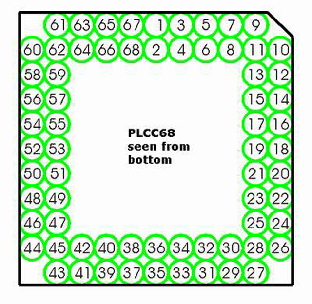
Something bothers me about that datasheet MichaelM mentioned... although this datasheet is extremely informative, the pin assignments are rotated 180 degrees from expected when looking at the socket's from the top (as if you could see through the socket). Why is that so, and wouldn't that throw someone off who wasn't paying close attention to the datasheet?

https://www.mill-max.com/assets/new_pro ... 43-145.pdf

Additionally, various other datasheets that I've found seem to expect a hole size of approximately 0.8 millimeters, which is smaller than the 0.036 inches (0.88 mm) suggested here. For the part I developed in DipTrace, I used 0.8 millimeters for the hole size and 1.1 mm for the pad size... I image 0.3 mm should be enough pad space.

Not sure if the silk screen will even be visible when all is said and done, however :P.


Top
 Profile  
Reply with quote  
PostPosted: Sat Mar 08, 2014 6:12 am 
Offline
User avatar

Joined: Fri Aug 30, 2002 1:09 am
Posts: 8460
Location: Southern California
It's normal to view the ICs (and other parts) from the top, not the bottom. I like to actually measure the pins and make the hole the smallest it can be while allowing for tolerances on the pins, drilling, and plating. I usually make the pad an extra .010" per side. I'm always looking for greater density though, and I never use the standard supplied library parts. When we were still doing a lot of thru-hole, IC pins were usually getting a .030" hole and .050" pad (allowing three traces between pins that are on .100" centers), and some things got .025" holes and .045" pads. Some things had to go bigger of course, like pin-header pins which were .025" square posts which are .035" across the corners, plus tolerances, so they got .040" holes and .060" pads.

I mostly keep the CAD reading out in thousandths of inches. It can read out in mm, but they go in increments that show it's still really keeping it all in thousandths of an inch internally. Recently manufacturers have been specifying things in mm more and more. (It's probably half and half now.) Since I keep a manilla folder with all the papers for every project anyway, I put a printout of all the special parts' dimensions and recommended land patterns in it, and write the inch dimensions next to the mm.

_________________
http://WilsonMinesCo.com/ lots of 6502 resources
The "second front page" is http://wilsonminesco.com/links.html .
What's an additional VIA among friends, anyhow?


Top
 Profile  
Reply with quote  
PostPosted: Sat Mar 08, 2014 8:29 am 
Offline
User avatar

Joined: Thu May 28, 2009 9:46 pm
Posts: 8232
Location: Midwestern USA
GARTHWILSON wrote:
It's normal to view the ICs (and other parts) from the top, not the bottom. I like to actually measure the pins and make the hole the smallest it can be while allowing for tolerances on the pins, drilling, and plating. I usually make the pad an extra .010" per side.

Same here. Too small a pad can result in it separating from the PCB while soldering. Too large a hole can sometimes lead to bad solder joints.

_________________
x86?  We ain't got no x86.  We don't NEED no stinking x86!


Top
 Profile  
Reply with quote  
PostPosted: Sat Mar 08, 2014 8:52 am 
Offline
User avatar

Joined: Fri Aug 30, 2002 1:09 am
Posts: 8460
Location: Southern California
I've never had any problems soldering from too small of a pad, but you definitely don't want any drill break-out on the side of the pad that has a trace coming to it, due to the drilling not being perfectly accurate and the bit getting kind of dull before it's replaced. (This is a reason for teardropping.) Also, one of the principals at a board house we used to use told me that the pad around the hole is important for getting a good plate-thru with kind of a rivet effect. Remember that the hole starts out bigger before it's plated, so with the extra size there plus the drilling inacuracy tolerance and the possibility of the bit not being new, you want to make sure there's still some pad ring all the way around the hole that the thru-plating can anchor to securely. When they give a copy of the company's whole thick quality manual, you find out more than you wanted to know about PCB manufacture.

_________________
http://WilsonMinesCo.com/ lots of 6502 resources
The "second front page" is http://wilsonminesco.com/links.html .
What's an additional VIA among friends, anyhow?


Top
 Profile  
Reply with quote  
Display posts from previous:  Sort by  
Post new topic Reply to topic  [ 9 posts ] 

All times are UTC


Who is online

Users browsing this forum: No registered users and 4 guests


You cannot post new topics in this forum
You cannot reply to topics in this forum
You cannot edit your posts in this forum
You cannot delete your posts in this forum
You cannot post attachments in this forum

Search for:
Jump to: