6502.org Forum  Projects  Code  Documents  Tools  Forum
It is currently Mon May 06, 2024 5:50 am

All times are UTC


Post new topic Reply to topic  [ 7 posts ] 
Author Message
PostPosted: Thu Oct 31, 2013 7:44 pm 
Offline

Joined: Mon Nov 11, 2002 6:53 pm
Posts: 79
Location: Seattle
Hi All,

While I've successfully hand-routed a number of smaller boards, my latest board has about 300 pins (including an 84-PLCC FPGA). The only way I manage to successfully route 'larger' boards is to use X/Y ( see http://www.ami.ac.uk/courses/ami4809_pcd/unit_01/images/pcd_ipcbt_imgaj.gif as an example) routing which, while effective, doesn't really look that great IMO. I usually flood-fill the bottom and make that the ground plane which tends to work (reasonably) well.

Anyone have any advice how to 'properly' route other than practice makes perfect? The 84-pin PLCC in particular gave me some headaches. Ironically, SMT boards seem much easier to route but a bitch to solder. Pick your poison I suppose :-)


Yvo


Top
 Profile  
Reply with quote  
PostPosted: Thu Oct 31, 2013 10:11 pm 
Offline
User avatar

Joined: Fri Aug 30, 2002 1:09 am
Posts: 8432
Location: Southern California
Flood-filling does not qualify for a ground plane in digital work unless you use a ton of vias where lines on opposite sides cross to keep the ground return paths right close to the signal lines that they correspond to. The behavior at the high frequencies involved in the edge rates is entirely different from what goes on in audio. I've looked for good diagrams online to post but have not had much success. I guess I'll have to scan ones in paper magazine articles I've kept, or draw my own. Fortunately, on a board the size of the one you show, you probably won't have any trouble making it work-- it just would not pass the FCC RF-radiation emission tests for marketing it commercially.

The X/Y characteristic you refer to is normal for boards having two signal layers. Near the edges, the X & Y are frequently not really perpendicular to each other like they are in the middle. After getting it routed, you can do via minimization. There's no need to keep lines at exactly 0° and 90°, or even 45°, so you can use whatever angles yield shorter, more-direct paths.

As for practice, if you be a perfectionist and keep working on tiny improvements after the design is basically done, I think you'll find more and more that you can apply to the next design. Board manufacturers also have limitations as to what does and does not present manufacturing problems, but it seems like we don't have to worry about those as much now as we did 15-25 years ago.

_________________
http://WilsonMinesCo.com/ lots of 6502 resources
The "second front page" is http://wilsonminesco.com/links.html .
What's an additional VIA among friends, anyhow?


Top
 Profile  
Reply with quote  
PostPosted: Fri Nov 01, 2013 7:12 am 
Offline
User avatar

Joined: Tue Nov 16, 2010 8:00 am
Posts: 2353
Location: Gouda, The Netherlands
For 2 layer boards, I always put a filled ground plane on both sides, and add plenty of vias to connect them together.

As far as X/Y routing, I do mostly surface mount parts, so generally, I try to route as much as possible on the component layer, and try to keep the traces on the bottom layer short. Here's an image from the board I'm currently working on. It's got a 6502 in a socket, SRAM, and FPGA. It's not finished (power isn't connected for example, and so are a bunch of control signals between 6502 and FPGA), but it shows work in progress. Note that I fully exploit the pin swap capabilities of the FPGA to avoid vias.
Attachment:
route1.PNG
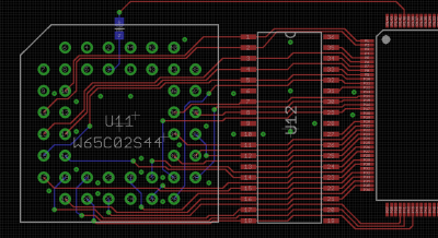
route1.PNG [ 61.31 KiB | Viewed 919 times ]


Here's the top + ground pour:
Attachment:
route2.PNG
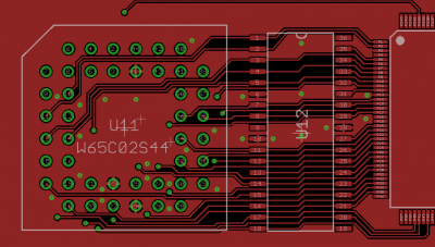
route2.PNG [ 42.52 KiB | Viewed 919 times ]

And the bottom:
Attachment:
route3.PNG
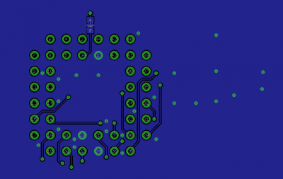
route3.PNG [ 25.24 KiB | Viewed 919 times ]


Note that the bottom looks empty now, but the power nets haven't been drawn yet. I do make an effort to keep the traces surrounded by ground as much as possible, avoiding to cut up the ground plane with long traces.


Top
 Profile  
Reply with quote  
PostPosted: Fri Nov 01, 2013 4:37 pm 
Offline

Joined: Mon Nov 11, 2002 6:53 pm
Posts: 79
Location: Seattle
Thanks for the reply guys!

The board in question is 5x5 inches and meh, looks alright. I'll post a picture when I get home later if you guys are interested. The wire-wrapped arcade board I did would be a b*tch to route but if you look at some of the early arcade boards, most of them were really, really well done.

Anyway, I'll take you guys' advice to heart! Thanks!

Yvo


Top
 Profile  
Reply with quote  
PostPosted: Fri Nov 01, 2013 4:46 pm 
Offline
User avatar

Joined: Tue Nov 16, 2010 8:00 am
Posts: 2353
Location: Gouda, The Netherlands
Another thing is to check exactly what the design rules are, and setting your PCB software up for that. For instance, the place where I have my PCBs made can do 6 mil trace/clearance for the standard price, and if the pads aren't too big, that allows 3 wires between 100 mil pads. Little things like that can make a big difference.


Top
 Profile  
Reply with quote  
PostPosted: Fri Nov 01, 2013 11:48 pm 
Offline

Joined: Mon Nov 11, 2002 6:53 pm
Posts: 79
Location: Seattle
Yup. Even though most places handle 6mil trace/clearance I never go down that low. I've got plenty of boards from places that messed up on clearance and what not. I tend to use quite a lot of clearance and generally try to route (for 100mil spacing anyway) only one trace in-between.

For SMT on the other hand, usually go down to about 12...

Yvo


Top
 Profile  
Reply with quote  
PostPosted: Sat Nov 02, 2013 6:39 am 
Offline
User avatar

Joined: Tue Nov 16, 2010 8:00 am
Posts: 2353
Location: Gouda, The Netherlands
Where I order my boards (eurocircuits.com), all of them are electrically tested before shipping. Any boards that fail the test are quickly replaced. That doesn't mean I use 6 mil traces all the time. If possible, I use 12, 10 or 8 mil traces, depending on the density of the board. But if the board requires it, I have gone down to 6 mil trace/clearance, and never had any problems.

Here's another board I had made at the same place. It's got 6 layers, 4 mil trace/clearance and 6 mil (0.15 mm) finished hole. I didn't design it myself, though.
Attachment:
jig.PNG
jig.PNG [ 82.54 KiB | Viewed 873 times ]


Top
 Profile  
Reply with quote  
Display posts from previous:  Sort by  
Post new topic Reply to topic  [ 7 posts ] 

All times are UTC


Who is online

Users browsing this forum: Google [Bot] and 3 guests


You cannot post new topics in this forum
You cannot reply to topics in this forum
You cannot edit your posts in this forum
You cannot delete your posts in this forum
You cannot post attachments in this forum

Search for:
Jump to: