So I think I have my first draft for a memory map and the chip select logic worked out. If I might run it by the group -
Chips: WDC65c02, 62256-80 RAM (32 Kb), NXP 2692A UART, VIA 65c22N, 2 x 28C64-150 EEPROM (each 8 Kb, two distinct chips so one socket can be used as a EEPROM programmer).
Rough map:
0000:7FFF  RAM
8000:      start of NXP 2692A
A000:      start of VIA 65c22N
C000:DFFF  ROM 2 (EEPROM socket)
E000:FFFF  ROM 1 (Bios, Monitor)
Since we are on 8k segments, the pin table only requires A15, A14, A13, as well as Phi2 for RAM. Ignoring that chip select lines are low for the moment, because it hurts my brain to do both steps at once, that gives us:
Phi2    A15    A14     A13
  1      0      x       x      RAM
  x      1      0       0      NXP
  x      1      0       1      VIA
  x      1      1       0      ROM 2
  x      1      1       1      ROM 1
Again, the result will have to be flipped for the actual chip select signals, which are low.
Now I've worked out that I could use four 3-line NAND gates and four 2-line NAND gates (three of them for negating signals, one for Phi2/A15 to RAM). Unfortunately, the only available 3-line NAND package seems to be the triple 3-line NAND 74HC10, which means I would need two of these chips (and one 74HC132 four 2-line NAND Schmitt trigger). That's three ICs in all. Unfortunately, the 74HC10 doesn't seem to have a Schmitt trigger. Worse, I don't think the design will call for a more 3-line NAND gates, so two-thirds of one 74HC10 would be wasted. That's not elegant.
However, looking at the bit table, I am wondering about a different approach.
1. For the RAM, invert A15 with a NAND, and NAND that with Phi2, as before. That's half of a 74HC132. I should be able to use the other half later -- one NAND will be needed with the reset button for the Schmitt trigger, for instance.
2. Now, for the other chips, use a 2-to-4 line decoder (half of a 74HC139), and NAND each of its output lines with A15, using up a full 74HC132. Three chips as well, but the output will be Schmitt triggered ("schmitted"?). The second half of the 74HC139 could be used for something in combination with the VIA or NXP, if only to drive LEDs (my kids love LEDs, and it looks like I'll be putting them in, like it or not). I'll figure that out later.
What I'm not sure about, though: The datasheets give a propagation delay for the 3-line NAND 74HC10 of 9 ns and 11 ns for the 2-to-4 74HC139. I have no feeling for how important those 2 ns are in the real-world -- any guidance on this? I'm planning to run everything low-speed, with anything above 1 MHz "nice to have".
So that's the plan so far. I'd be grateful for any corrections or suggestions, of course ...
Memory map design with 2-to-4 line decoder?
-
ElEctric_EyE
- Posts: 3260
- Joined: 02 Mar 2009
- Location: OH, USA
Re: Memory map design with 2-to-4 line decoder?
You could make your address decoding even easier. Put A13-A15 into a 3-8 decoder & phase2 into one of the active high enables. That divides the entire 64K into 8K chunks like you have. You will need each the top 4 selects from the decoder for each of your I/O & ROMs. The lower 4 selects you would logic 'OR' or 'NOR' for your RAM depending on if you're using the active low or active high enable.
Note though, if you want higher speed later on, your phase 2 should be decoded as close to the device as possible, i.e. last in the logic path. Have a look at BDD's POC v.1 schematic. Notice the signals he uses for decoding the RAM vs. ROM.
The 2ns is not what to be concerned about. Look at the max delay after adding all your delays in the logic path + access times of the device. This will give you a ballpark when you start to push max speeds.
Re: Memory map design with 2-to-4 line decoder?
Alternatively, you could check if Daryl Rictor has a pre-programmed address decoder GAL available: http://sbc.rictor.org/decoder.html. I'm not sure what the speed of this would be, but it looks like a simpler solution than the ones you describe.

Re: Memory map design with 2-to-4 line decoder?
rwiker wrote:
Alternatively, you could check if Daryl Rictor has a pre-programmed address decoder GAL available: http://sbc.rictor.org/decoder.html. I'm not sure what the speed of this would be, but it looks like a simpler solution than the ones you describe.
The chips are 15ns chips so should work easily up to and beyond a 14MHz clock. $9 plus postage.
Let me know if you are interested.
Daryl
Please visit my website -> https://sbc.rictor.org/
-
BigDumbDinosaur

- Posts: 9425
- Joined: 28 May 2009
- Location: Midwestern USA (JB Pritzker’s dystopia)
- Contact:
Re: Memory map design with 2-to-4 line decoder?
scotws wrote:
So I think I have my first draft for a memory map and the chip select logic worked out. If I might run it by the group -
Chips: WDC65c02, 62256-80 RAM (32 Kb), NXP 2692A UART, VIA 65c22N, 2 x 28C64-150 EEPROM (each 8 Kb, two distinct chips so one socket can be used as a EEPROM programmer).
Rough map:
Since we are on 8k segments, the pin table only requires A15, A14, A13, as well as Phi2 for RAM. Ignoring that chip select lines are low for the moment, because it hurts my brain to do both steps at once, that gives us:
Again, the result will have to be flipped for the actual chip select signals, which are low.
Chips: WDC65c02, 62256-80 RAM (32 Kb), NXP 2692A UART, VIA 65c22N, 2 x 28C64-150 EEPROM (each 8 Kb, two distinct chips so one socket can be used as a EEPROM programmer).
Rough map:
Code: Select all
0000:7FFF RAM
8000: start of NXP 2692A
A000: start of VIA 65c22N
C000:DFFF ROM 2 (EEPROM socket)
E000:FFFF ROM 1 (Bios, Monitor)Code: Select all
Phi2 A15 A14 A13
1 0 x x RAM
x 1 0 0 NXP
x 1 0 1 VIA
x 1 1 0 ROM 2
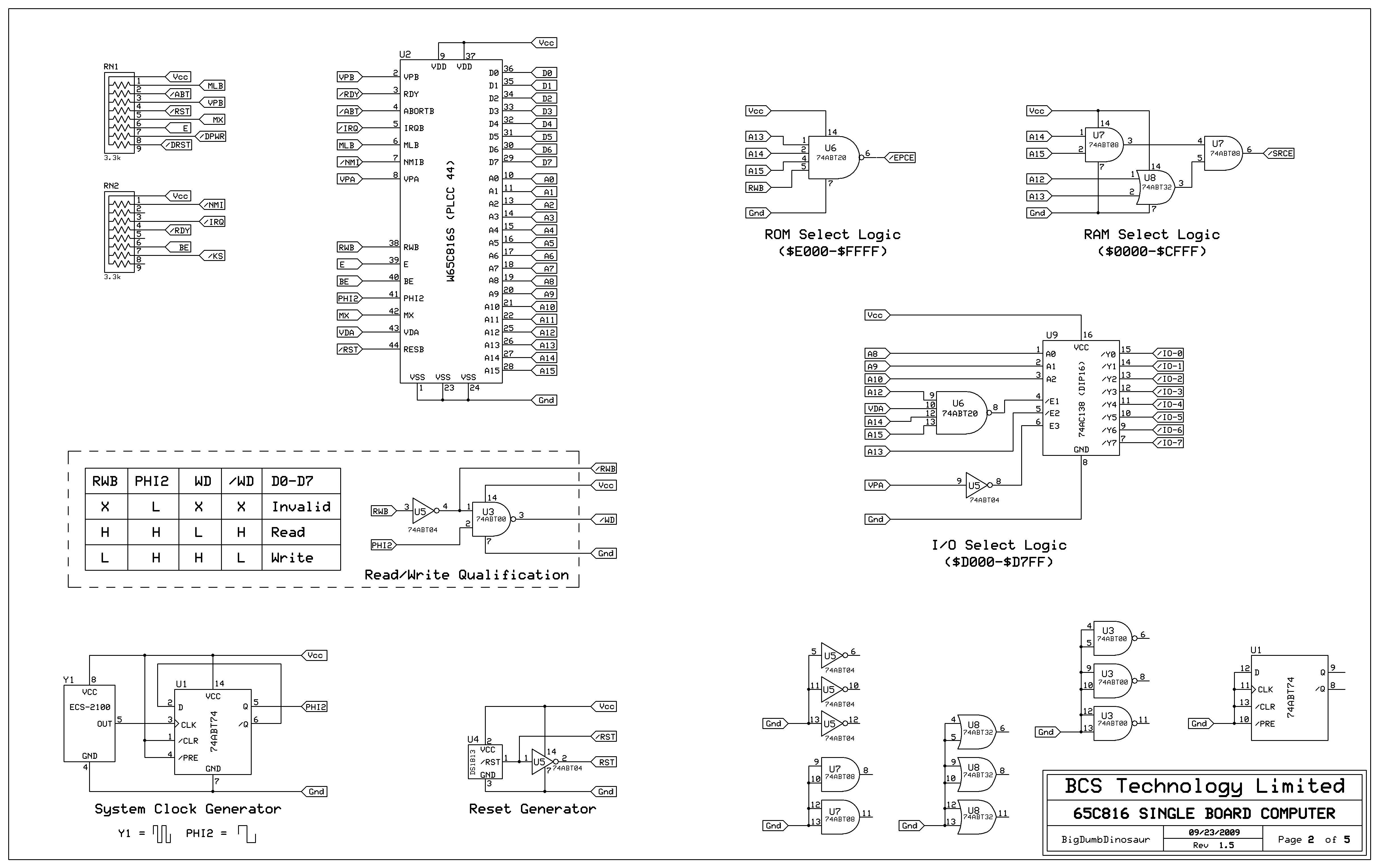
x 1 1 1 ROM 1What's Ø2 doing in there? You should not be qualifying decodes with Ø2. Use Ø2 to qualify read/write only. The 65C22, in particular must be selected prior to Ø2 going high. This is clearly spelled out in the timing diagrams. You want your chip selects ready before Ø2 goes high to give the selected device plenty of time to get ready for access. Using Ø2 as a qualifying signal "throws away" valuable time, since the device won't be ready until some time after Ø2 has gone high and the MPU is expecting access to the device.
In the same vein, qualify RWB with Ø2 so /OE (output enable) or /WE (write enable) of the selected device are not asserted when Ø2 is low. Failure to do so with RAM and I/O devices may cause data corruption. See attached schematic.
As for selecting devices, have you looked at the 74AC138 3-8 decoder (data sheet attached)? I think that is all you would need for this application. It has eight low-true outputs that can drive your devices' /CS inputs. BTW, best to use 74AC instead of 74HC logic.
Quote:
What I'm not sure about, though: The datasheets give a propagation delay for the 3-line NAND 74HC10 of 9 ns and 11 ns for the 2-to-4 74HC139. I have no feeling for how important those 2 ns are in the real-world -- any guidance on this? I'm planning to run everything low-speed, with anything above 1 MHz "nice to have".
Propagation time is cumulative, so you can quickly "run out" of time if too much logic is required to decoded addresses into chip selects. The 74AC138 decoder has a prop time of as little as 3ns at 5 volts and no more than 11ns worst-case. If you can figure out how to integrate the '138 into your design as the primary logic then your circuit's speed will be mostly limited by how well you do your assembly.
The 65C22N is an open-drain IRQ part designed to replace the old NMOS equivalent. It has current limiting resistors on the output pins. You may wish to consider the 65C22S. However, it has a totem-pole IRQ output, so it will have to be isolated from the rest of the IRQ circuit with Schottky diode, since the 2692 has an open-drain IRQ output.
- Read/Write Qualification with Ø2
x86? We ain't got no x86. We don't NEED no stinking x86!
Re: Memory map design with 2-to-4 line decoder?
Thanks for the feedback everybody. I'm struggling a bit with timing diagrams, because so far, I could just mentally connect the little black boxes with little black lines. Working on it.
My "local" internet parts supplier only has the AC stuff as SMC, and I'm looking to wirewrap this one -- I have a mild case of essential tremor, so precise work with fiddly small bits can be frustrating, including soldering. Another thing I'm testing with this first project.
I actually have the 74HC237 variant of a 3-to-8 (has a latch) and have been messing around with it. However, wouldn't that just add another station to the RAM selection? I'd have to "catch" the four lines to that segment of of the memory with a four-line AND chip, so I'd have at least two chips in the way. If I just use A15 for the RAM and a 2-to-4 for the rest, that should be a step less for the RAM (see attachment).
That's precisely why I was going to go with the N, it looks easier to handle.
Daryl, thanks for the offer, I've, well, drooled over your whole page there. My idea is do this one the hard way to make sure I actually understand what's going on (work in progress, obviously). The second machine would be one where I'd be looking at all such things. You're bookmarked .
.
BigDumbDinosaur wrote:
As for selecting devices, have you looked at the 74AC138 3-8 decoder (data sheet attached)? I think that is all you would need for this application.
I actually have the 74HC237 variant of a 3-to-8 (has a latch) and have been messing around with it. However, wouldn't that just add another station to the RAM selection? I'd have to "catch" the four lines to that segment of of the memory with a four-line AND chip, so I'd have at least two chips in the way. If I just use A15 for the RAM and a 2-to-4 for the rest, that should be a step less for the RAM (see attachment).
BigDumbDinosaur wrote:
You may wish to consider the 65C22S. However, it has a totem-pole IRQ output, so it will have to be isolated from the rest of the IRQ circuit with Schottky diode, since the 2692 has an open-drain IRQ output.
Daryl, thanks for the offer, I've, well, drooled over your whole page there. My idea is do this one the hard way to make sure I actually understand what's going on (work in progress, obviously). The second machine would be one where I'd be looking at all such things. You're bookmarked
- Attachments
-
Re: Memory map design with 2-to-4 line decoder?
scotws wrote:
Daryl, thanks for the offer, I've, well, drooled over your whole page there. My idea is do this one the hard way to make sure I actually understand what's going on (work in progress, obviously). The second machine would be one where I'd be looking at all such things. You're bookmarked .
Daryl
Please visit my website -> https://sbc.rictor.org/

Re: Memory map design with 2-to-4 line decoder?
scotws
You can do what you wish with just 1 74HC139 and a single inverter.
Note that the 74HC139 outputs go low when selected and the CS' or CE' pins of the devices you wish to select need to go low when selected - exactly what we need for simple connections.
Connect A15 directly to the RAM CS' pin. This enables the RAM whenever A15 is low, ie for 0000 - 7FFF.
Invert A15 and feed it to the enable input of the 74HC139. Connect the A & B inputs of the 74HC139 to A13 and A14. The outputs of the 74HC139 can connect directly to the CS pins of your ROMs and IO devices. This decodes 8000 - FFFF into 8k chunks like you want.
Note that the Phase2 signal is NOT included in the address decoding. It is not needed. Leaving out Phase2 gives the memory and I/O devices a longer time period for chip selection - not a major problem with modern devices at 1MHz but it becomes significant at higher speeds. Also, the 65C22 needs its chip select to become active before Phase2 goes high, so you cannot include Phase2 in a decoder that selects a 65C22.
Use the other half of the 74HC139 to decode the Phase2 and R/W' signals from the CPU. Of the four outputs, one is READ' (when Phase2 and R/W' are both high) and one is WRITE' (when Phase2 is high and R/W' is low). Connect the READ' output to the OE' pins of your RAM and ROMs. Connect the WRITE' output to the WE' pin of the RAM chip. This enables output from the device when the 65C02 is performing a read and enables a write to the RAM when the 65C02 is performing a write.
I couldn't find a data sheet for the NXP2692A you mentioned. I assume it's a DUART equivilant to the SCC2692. If that's the case, the decoded READ' signal from the 74HC139 connects to the RDN input and the decoded WRITE' signal from the 74HC139 connects to the WDN input.
Don't worry about the propagation delays of 74HC logic if you are only running at 1MHz - at this speed 74HC logic is far more than fast enough. It's only when you get to higher speeds that propagation delays become something to worry about. Using an inverter and a 74HC139 as above, you should have no problems at 4MHz.
Shift to the left,
Shift to the right,
Mask in, Mask Out,
BYTE! BYTE! BYTE!
Shift to the right,
Mask in, Mask Out,
BYTE! BYTE! BYTE!
-
BigDumbDinosaur
- Posts: 9425
- Joined: 28 May 2009
- Location: Midwestern USA (JB Pritzker’s dystopia)
- Contact:
Re: Memory map design with 2-to-4 line decoder?
PaulF wrote:
Note that the Phase2 signal is NOT included in the address decoding. It is not needed. Leaving out Phase2 gives the memory and I/O devices a longer time period for chip selection - not a major problem with modern devices at 1MHz but it becomes significant at higher speeds. Also, the 65C22 needs its chip select to become active before Phase2 goes high, so you cannot include Phase2 in a decoder that selects a 65C22.
I explained all that in an earlier post.
Quote:
I couldn't find a data sheet for the NXP2692A you mentioned. I assume it's a DUART equivilant to the SCC2692. If that's the case, the decoded READ' signal from the 74HC139 connects to the RDN input and the decoded WRITE' signal from the 74HC139 connects to the WDN input.
NXP is the old Phillips semiconductor line. Back when it was Phillips everything was SCCxxxx.
See attached 2692 data sheets. I also included the 2692's big brother, the 2698 octart (eight UARTs in on package).
Also, pay attention to how you access the 2692's configuration registers. There's a timing issue that has to be observed, which can be accomplished in software.
x86? We ain't got no x86. We don't NEED no stinking x86!
Re: Memory map design with 2-to-4 line decoder?
Hi Paul,
Ay, thanks for all the detail! I won't even post what I had been working on for R/W' and stuff -- mentally, I still have this tendency to try to reduce everything to AND and NOT first before thinking, gee, there is half of a 2-to-4 over here ...
I've included a sketch of how I understood your description (pin numbers need to be re-checked, will do that when I'm fully awake). Don't I need two inverters, a second one on the VIA for CS1 (CS2 is low already)? I connected the R/W' on the VIA directly to the R/W' of the 65c02 as per Garth's tutorial example.
Thanks again. I'll try to get my hands on a '139 next week and breadboard a test.
Wow, what a monster. What would this be for, terminals?
PaulF wrote:
You can do what you wish with just 1 74HC139 and a single inverter.
I've included a sketch of how I understood your description (pin numbers need to be re-checked, will do that when I'm fully awake). Don't I need two inverters, a second one on the VIA for CS1 (CS2 is low already)? I connected the R/W' on the VIA directly to the R/W' of the 65c02 as per Garth's tutorial example.
Thanks again. I'll try to get my hands on a '139 next week and breadboard a test.
BigDumbDinosaur wrote:
I also included the 2692's big brother, the 2698 octart (eight UARTs in on package).
- Attachments
-
-
GARTHWILSON

- Forum Moderator
- Posts: 8773
- Joined: 30 Aug 2002
- Location: Southern California
- Contact:
Re: Memory map design with 2-to-4 line decoder?
Quote:
Don't I need two inverters, a second one on the VIA for CS1 (CS2 is low already)?
http://WilsonMinesCo.com/ lots of 6502 resources
The "second front page" is http://wilsonminesco.com/links.html .
What's an additional VIA among friends, anyhow?
The "second front page" is http://wilsonminesco.com/links.html .
What's an additional VIA among friends, anyhow?
Re: Memory map design with 2-to-4 line decoder?
I've noticed a mistake on the diagram you posted. Only E1 on the 74HC139 should be connected to the inverted A15. E2 should be connected directly to 0V. You want this section of the 74HC139 to be permanently enabled. As shown, it won't generate READ' and WRITE' signals when A15 is low, so you won't be able to read from or write to RAM!
As Garth Wilson says, you don't need the inverter to drive CS1 on the 65C22. Just tie this pin to +5V
Otherwise, you have correctly interpreted my ramblings. Hope it helps and good luck!
As Garth Wilson says, you don't need the inverter to drive CS1 on the 65C22. Just tie this pin to +5V
Otherwise, you have correctly interpreted my ramblings. Hope it helps and good luck!
Shift to the left,
Shift to the right,
Mask in, Mask Out,
BYTE! BYTE! BYTE!
Shift to the right,
Mask in, Mask Out,
BYTE! BYTE! BYTE!
-
BigDumbDinosaur
- Posts: 9425
- Joined: 28 May 2009
- Location: Midwestern USA (JB Pritzker’s dystopia)
- Contact:
Re: Memory map design with 2-to-4 line decoder?
scotws wrote:
BigDumbDinosaur wrote:
I also included the 2692's big brother, the 2698 octart (eight UARTs in one package).
Back when dumb terminals (e.g., the venerable WYSE 60) were in widespread use, a port concentrator or terminal server was used to connect multiple terminals to a single I/O port on the (mini)computer. The 2698 was often used in these concentrators to help keep the chip count under control. For each 2698, a total of eight 1488 and eight 1489 line drivers was required. There is at least one company that sells an eight port TIA-232 plug-in card for PCs that uses the 2698, but I don't recall anymore who it is or where one might acquire one.
The 2698's programming model is exactly the same as that of the 2692, as the 2698 is functionally four 2692s in a PLCC84 package. There are just a few more channels to configure and one or two extra (!) interrupt sources to service.
Twenty-some years ago I worked on a terminal server project that used the 2698 and a 65C02 (I wrote the firmware). Seven of the serial ports were connected to terminals, and the remaining port was an I/O path to the minicomputer (a Point 4 unit)—that port ran at 115.2 Kbps CBAT. Up to eight concentrators could be attached to the mini, supporting up to 56 serial devices. The 'C02 in each concentrator was a busy fellow servicing all those interrupts.
See below for a little 2692 code to get you started. These defs will also work with the 26C92 but would be incomplete in some respects.
Code: Select all
;================================================================================
;
;NXP2692 DUAL ACIA DEFINITIONS
;
nc_92a   =2                    ;number of channels
nr_92a   =8                    ;registers per channel
nr_2692  =nr_92a*nc_92a        ;total registers
;
;
;	register offsets...
;
dr_acr   =%0100                ;auxiliary control register (W)...
;
;	xxxxxxxx
;	||||||||
;	|||||||+———> 1: enable IP0 IRQ
;	||||||+————> 1: enable IP1 IRQ
;	|||||+—————> 1: enable IP2 IRQ
;	||||+——————> 1: enable IP3 IRQ
;	|+++———————> C/T setup:
;	|
;	|            654  Mode     Source
;	|            ———————————————————————————————
;	|            000  counter  IP2
;	|            001  counter  TxD Ch 1 1X clock
;	|            010  counter  TxD Ch 2 1X clock
;	|            011  counter  Xtal/16
;	|            100  timer    IP2
;	|            101  timer    IP2/16
;	|            110  timer    Xtal
;	|            111  timer    Xtal/16
;	|            ———————————————————————————————
;	|
;	+——————————> 0: select BRG set #1 (38.4k max)
;	             1: select BRG set #2 (19.2k max)
;
dr_cra   =%0010                ;ch A command (W)...
;
;	xxxxxxxx
;	||||||||
;	||||||++———> 00: no operation
;	||||||       01: enable receiver
;	||||||       10: disable receiver
;	||||||       11: illegal operation
;	||||++—————> 00: no operation
;	||||         01: enable transmitter
;	||||         10: disable transmitter
;	||||         11: illegal operation
;	++++———————> 0000: no operation
;	             0001: reset mode select to MR1
;	             0010: reset & disable receiver
;	             0011: reset & disable transmitter
;	             0100: reset error status
;	             0101: reset break IRQ
;	             0110: start TxD break
;	             0111: stop TxD break
;	             1000: assert RTS
;	             1001: deassert RTS
;	             1010: enable C/T timeout mode
;	             1011: undefined
;	             1100: disable C/T timeout mode
;	             1101: undefined
;	             1110: standby power mode
;	             1111: normal power mode
;
dr_crb   =%1010                ;ch B command (W)...
;
;	xxxxxxxx
;	||||||||
;	||||||++———> 00: no operation
;	||||||       01: enable receiver
;	||||||       10: disable receiver
;	||||||       11: illegal operation
;	||||++—————> 00: no operation
;	||||         01: enable transmitter
;	||||         10: disable transmitter
;	||||         11: illegal operation
;	++++———————> 0000: no operation
;	             0001: reset mode select to MR1
;	             0010: reset & disable receiver
;	             0011: reset & disable transmitter
;	             0100: reset error status
;	             0101: reset break IRQ
;	             0110: start TxD break
;	             0111: stop TxD break
;	             1000: assert RTS
;	             1001: deassert RTS
;	             1010: enable C/T timeout mode
;	             1011: undefined
;	             1100: disable C/T timeout mode
;	             1101: undefined
;	             1110: undefined
;	             1111: undefined
;
dr_crlr  =%0111                ;C/T LSB preset (W)
dr_crur  =%0110                ;C/T MSB preset (W)
dr_csra  =%0001                ;ch A clock select (W)...
;
;	xxxxxxxx
;	||||||||
;	||||++++———> TxD baud rate & BRG source
;	++++———————> RxD baud rate & BRG source
;
dr_csrb  =%1001                ;ch B clock select (W)...
;
;	xxxxxxxx
;	||||||||
;	||||++++———> TxD baud rate & BRG source
;	++++———————> RxD baud rate & BRG source
;
dr_ctl   =dr_crlr              ;C/T LSB value (R)
dr_ctu   =dr_crur              ;C/T MSB value (R)
dr_imr   =%0101                ;interrupt enable mask (W)...
;
;	xxxxxxxx
;	||||||||
;	|||||||+———> 1: enable ch A THR ready
;	||||||+————> 1: enable ch A RHR ready/FIFO full
;	|||||+—————> 1: enable ch A change in break
;	||||+——————> 1: enable C/T ready
;	|||+———————> 1: enable ch B THR ready
;	||+————————> 1: enable ch B RHR ready/FIFO full
;	|+—————————> 1: enable ch B change in break
;	+——————————> 1: enable IP0-IP3 state change
;
dr_ipcr  =dr_acr               ;input port change (R)
dr_ipsr  =dr_opcr              ;input port status (R)
dr_isr   =dr_imr               ;interrupt status (R)...
;
;	xxxxxxxx
;	||||||||
;	|||||||+———> 1: ch A THR ready
;	||||||+————> 1: ch A RHR ready/FIFO full
;	|||||+—————> 1: ch A change in break
;	||||+——————> 1: C/T ready
;	|||+———————> 1: ch B THR ready
;	||+————————> 1: ch B RHR ready/FIFO full
;	|+—————————> 1: ch B change in break
;	+——————————> 1: IP0-IP3 state change
;
dr_msra  =%0000                ;ch A mode select...
;
;	xxxxxxxx———> mode 1 settings
;	||||||||
;	||||||++———> data format:  00: 5 bit
;	||||||                     01: 6 bit
;	||||||                     10: 7 bit
;	||||||                     11: 8 bit
;	|||||+—————> parity type:   0: even
;	|||||                       1: odd
;	|||++——————> parity mode:  00: check
;	|||                        01: force
;	|||                        10: don't check
;	|||                        11: multidrop
;	||+————————> error mode:    0: character
;	||                          1: block
;	|+—————————> RxD IRQ mode:  0: RxD ready
;	|                           1: FIFO full
;	+——————————> RxD RTS mode:  0: off
;
;	xxxxxxxx———> mode 2 settings
;	||||||||
;	||||++++———> stop bit length
;	||||
;	|||+———————> TxD CTS mode:  0: off
;	|||                         1: on
;	||+————————> TxD RTS mode:  0: off
;	||                          1: on
;	++—————————> channel mode: 00: normal
;	                           01: auto echo
;	                           10: local loop
;	                           11: remote loop
;
dr_msrb  =%1000                ;ch B mode select...
;
;	——————————————————
;	mode 1 bit pattern
;	——————————————————
;
;	xxxxxxxx
;	||||||||
;	||||||++———> data format:  00: 5 bit
;	||||||                     01: 6 bit
;	||||||                     10: 7 bit
;	||||||                     11: 8 bit*
;	|||||+—————> parity type:   0: even*
;	|||||                       1: odd
;	|||++——————> parity mode:  00: check
;	|||                        01: force
;	|||                        10: don't check*
;	|||                        11: multidrop
;	||+————————> error mode:    0: character*
;	||                          1: block
;	|+—————————> RxD IRQ mode:  0: RxD ready*
;	|                           1: FIFO full
;	+——————————> RxD RTS mode:  0: off
;	                            1: on*
;	* = default setting
;
;	——————————————————
;	mode 2 bit pattern
;	——————————————————
;
;	xxxxxxxx
;	||||||||
;	||||++++———> stop bit length
;	||||
;	|||+———————> TxD CTS mode:  0: off
;	|||                         1: on
;	||+————————> TxD RTS mode:  0: off
;	||                          1: on
;	++—————————> channel mode: 00: normal
;	                           01: auto echo
;	                           10: local loop
;	                           11: remote loop
;
dr_opcr  =%1101                ;output port configuration (W)
dr_rctc  =dr_ropbc             ;stop C/T command (R)
dr_rhra  =dr_thra              ;ch A RxD holding (R)
dr_rhrb  =dr_thrb              ;ch B RxD holding (R)
dr_ropbc =%1111                ;reset output port bits command (W)
dr_rsrvd =%1100                ;reserved
dr_sctc  =dr_sopbc             ;start C/T command (R)
dr_sopbc =%1110                ;set output port bits command (W)
dr_sra   =dr_csra              ;ch A status (R)...
;
;	xxxxxxxx
;	||||||||
;	|||||||+———> 1: RxD ready for read
;	||||||+————> 1: RxD FIFO full
;	|||||+—————> 1: TxD ready for write
;	||||+——————> 1: TxD empty
;	|||+———————> 1: RxD overrun
;	||+————————> 1: parity error
;	|+—————————> 1: framing error
;	+——————————> 1: BRK received
;
dr_srb   =dr_csrb              ;ch B status (R)...
;
;	xxxxxxxx
;	||||||||
;	|||||||+———> 1: RxD ready for read
;	||||||+————> 1: RxD FIFO full
;	|||||+—————> 1: TxD ready for write
;	||||+——————> 1: TxD empty
;	|||+———————> 1: RxD overrun
;	||+————————> 1: parity error
;	|+—————————> 1: framing error
;	+——————————> 1: BRK received
;
dr_thra  =%0011                ;ch A TxD holding (W)
dr_thrb  =%1011                ;ch B TxD holding (W)
;
	.end
x86? We ain't got no x86. We don't NEED no stinking x86!
Re: Memory map design with 2-to-4 line decoder?
PaulF wrote:
As shown, it won't generate READ' and WRITE' signals when A15 is low, so you won't be able to read from or write to RAM!
- Attachments
-
-
Last edited by scotws on Thu Feb 21, 2013 9:27 pm, edited 1 time in total.
Re: Memory map design with 2-to-4 line decoder?
BigDumbDinosaur wrote:
See below for a little 2692 code to get you started. These defs will also work with the 26C92 but would be incomplete in some respects.