6502.org Forum  Projects  Code  Documents  Tools  Forum
It is currently Fri Apr 26, 2024 11:35 pm

All times are UTC


Post new topic Reply to topic  [ 91 posts ]  Go to page 1, 2, 3, 4, 5 ... 7  Next
Author Message
PostPosted: Sun Feb 10, 2013 8:51 am 
Offline
User avatar

Joined: Fri Dec 11, 2009 3:50 pm
Posts: 3346
Location: Ontario, Canada
Bus timing for 65c816 is potentially more challenging than timing for 65c02. Although address lines A15-A0 have the same job as on a 6502, D7-D0 carry extra activity. As noted in the data sheet, "The Data/Bank Address Bus pins provide both the Bank Address and Data. The bank address is present during the first half of a memory cycle, and the data value is read or written during the second half of the memory cycle." I started this thread because I thought it was worth discussing the details.

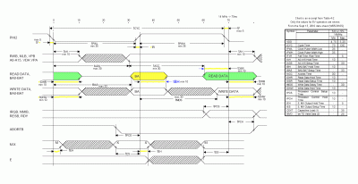
First, two diagrams. Below is my own edited version of Figure 4-1 from the '816 Data Sheet (Sept 2010 version). To put all the various delays in perspective I squeezed and stretched things so that the diagram is now approximately to scale along the horizontal axis.

Assuming a 70 ns cycle (14 MHz), WYSIWYG! :) WDC's original diagram has two errors of omission; my corrections are shown in blue (I added 2 missing arrowheads and the value name tBH). Proofreaders welcome. Also, from Table 4-2, I copied in the actual delays (in ns.) that pertain to 5V operation. The clock rise & fall times have not been adjusted to scale.
Attachment:
65816 timing.gif
65816 timing.gif [ 48.31 KiB | Viewed 13724 times ]

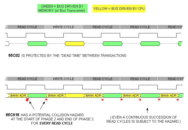
The next diagram (below) shows the extra activity on D7-D0, as compared to a 6502. D7-D0 are bidirectional, meaning that the CPU and the system board must both drive them -- but of course never simultaneously, which would amount to a collision (aka bus contention).
Attachment:
data bus activity for 6502 vs 65816.gif
data bus activity for 6502 vs 65816.gif [ 10.8 KiB | Viewed 13362 times ]

It's when the bus reverses direction that there's potential for a problem. A graceful reversal demands that the CPU release the bus before the memory or transceiver on the system board commences to drive it. Likewise the system board must release the bus before the CPU commences to drive it.

With 6502, it's easy. The bus never reverses direction except when read cycles are interspersed with writes. More to the point, neither the processor nor the system board (if it's properly designed) drives the data bus during Phase 2 low.

The "dead time" during 65c02 Phase 2 low is actually extremely valuable! It acts as a timing cushion that accommodates real-world variability -- for example, the tri-state enable & disable delays of the memory or transceiver that drives the bus, the delay of the glue logic in control of that, and the timing variability of the CPU's own internal bus driver. These delays can't be exactly predicted, and vary independently of one another. The dead time will be at its most brief when the device releasing is at its slowest and the device asserting is at its fastest. But the 6502 has plenty of wiggle room. The dead time is nominally 50% of the cycle, and won't get eaten up even after a margin is subtracted for variability in logic and tri-state delays.

With the '816, it's a stickier situation. Even in the case of successive read cyles, the bus must reverse direction. But really the crucial issue is...

  • in Phase 2 low the CPU drives the Bank Address onto the data bus
  • instantly thereafter, during Phase 2 high, memory drives data on the bus
  • instantly thereafter it's back to the CPU driving the Bank Address onto the data bus

Stated another way, the dead time is zero even before a margin is subtracted for variability in logic and tri-state delays. Of course the variability might trend in your favor, creating a dead time. But it equally might trend the other way and create bus contention. I'm not aware of any really good solution for this.

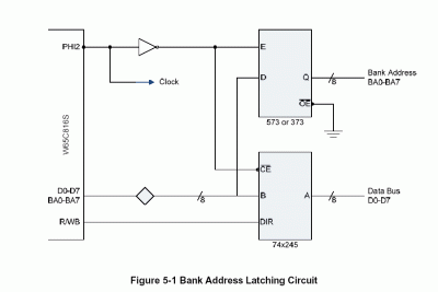
What I'd like to determine is how best to design for the '816. Here's Figure 5-1.
Attachment:
65816 Bank Address Latching Circuit.gif
65816 Bank Address Latching Circuit.gif [ 15.86 KiB | Viewed 13750 times ]
I'm sure this circuit has been used successfully many times, but it's somewhat vague. Is it safe to assume that, for the "74x245" bus transceiver, we can use anything from a 74LS245 to a 74BCT245? What if it's a CPLD or some other device that connects to D7-D0? How do we ensure that the bus enable and bus inhibit times are appropriate for avoiding bus collisions with the '816? Here's what we have to go on:
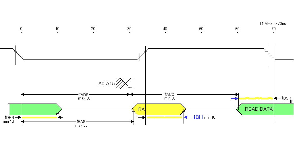
Attachment:
65816 bus assert-release.gif
65816 bus assert-release.gif [ 9.18 KiB | Viewed 13724 times ]

  • I think we can accept tBAS (max 33ns) as the maximum delay from Phase 2 low until the '816 asserts the bus. What's the minimum?
  • Likewise, tBH (min 10) can be interpreted as the minimum delay from Phase 2 high until the '816 releases the bus. What's the maximum?
  • tDHR (min 10) can be interpreted as the minimum delay from Phase 2 low until the system board releases the bus. What's the maximum?
  • As for the delay from Phase 2 high until the system board asserts the bus, none of the values in the diagram seems directly pertinent, either for maximum or minimum.

Is there something I've overlooked, or do these specifications fail to tell the whole story?

cheers,
Jeff

[Edits: 2 more missing specs noted in the last paragraph. Altered text and new "data bus activity" and to clarify contention issue.]

_________________
In 1988 my 65C02 got six new registers and 44 new full-speed instructions!
https://laughtonelectronics.com/Arcana/ ... mmary.html


Last edited by Dr Jefyll on Thu Dec 12, 2013 6:01 pm, edited 2 times in total.

Top
 Profile  
Reply with quote  
PostPosted: Sun Feb 10, 2013 1:33 pm 
Offline
User avatar

Joined: Fri Aug 30, 2002 1:09 am
Posts: 8428
Location: Southern California
Excellent, Jeff. Thanks. I emailed Bill Mensch many years ago about ambiguities in this part of the data sheet, showing, IIRC, that the part could meet the specifications and yet not work anywhere near as fast as the speed rating. He said in his response, again IIRC, that he didn't have the answer, but that the parts do work beyond their specified speed, and recommended that I experiment if I wanted better info. (Despite the way I make it sound here, he was very gracious about it but admitted he was not able to give definitive answers.) Since then I've had the ambition to experiment with delay lines like Data Delay Devices makes and move the timing of especially the 573's E input forward and back a ns or two at a time relative to the phase-2 to the rest of the system and watch the current (indicating bus contention) and see where the whole thing would run the fastest. There would be other timings that could be experimented with similarly. I never have done that though.

_________________
http://WilsonMinesCo.com/ lots of 6502 resources
The "second front page" is http://wilsonminesco.com/links.html .
What's an additional VIA among friends, anyhow?


Top
 Profile  
Reply with quote  
PostPosted: Sun Feb 10, 2013 4:42 pm 
Offline
User avatar

Joined: Fri Dec 11, 2009 3:50 pm
Posts: 3346
Location: Ontario, Canada
GARTHWILSON wrote:
I've had the ambition to experiment with delay lines [...] and watch the current (indicating bus contention) and see where the whole thing would run the fastest. [...] I never have done that though.
That's on my list of "someday" projects, too. <sigh> :roll:
GARTHWILSON wrote:
There would be other timings that could be experimented with similarly.
Yes, including the duty cycle on Phi2.
I wrote:
A graceful reversal demands that CPU release the bus before the transceiver on the system board commences to drive it, and vice versa
This is by no means just an '816 issue; there are other examples, including 8085, 8088 and 8086. I recall a case where a friend's employer had an 8086 design. It became obligatory to include bus transceivers to connect the EPROMs to the data bus, not because of insufficient drive current but because the EPROMs were too slow letting go of the bus.

Even in light of this, my speculation is that modern RAMs could be connected directly to the '816's D7-D0 -- ie, without a transceiver. But there would be benefits from including the transceiver anyway, such as relieving some of the capacitive loading seen by the CPU.

_________________
In 1988 my 65C02 got six new registers and 44 new full-speed instructions!
https://laughtonelectronics.com/Arcana/ ... mmary.html


Last edited by Dr Jefyll on Sun Feb 10, 2013 4:54 pm, edited 1 time in total.

Top
 Profile  
Reply with quote  
PostPosted: Sun Feb 10, 2013 4:51 pm 
Offline
User avatar

Joined: Fri Aug 30, 2002 9:02 pm
Posts: 1681
Location: Sacramento, CA
You have spent much more time studying this than I did Jeff - nice work!

On my SBC-3 & 4, I used a CPLD to manage the latching of the bank address. This was a simple latch, equivalent to the 74573. It was transparent during PHI2 low, and latched when PHI2 was high. I didn't bother with any delays or shifting of PHI2. This worked flawlessly up to and beyond 14MHz as long as my bus loading was light. With more devices on the bus, lower speeds (8-12MHZ) worked well. My CPLD's were typically 15ns Xilinx 95108's.

As far as managing the databus, the tri-state buffers used in the CPLD also used PHI2 & R/W in addition to the address decoding logic to select the CPU, Memory, or IO as needed. No special attention to the PHI2 edges were needed.

SBC-3 went one step further in using the PHI2 low period to perform video data transfer.

I cannot say it did not cause bus contention, but I can say it didn't affect the operation of my two systems.

Just my two cents.

Daryl

_________________
Please visit my website -> https://sbc.rictor.org/


Top
 Profile  
Reply with quote  
PostPosted: Tue Feb 12, 2013 3:18 am 
Offline
User avatar

Joined: Fri Dec 11, 2009 3:50 pm
Posts: 3346
Location: Ontario, Canada
In a different thread,
BigEd wrote:
The success of several projects in (almost) dropping in an 816 to an 02 design indicate that the address muxing onto the databus in the first half of the cycle may be no problem. Note that systems such as the Beeb and the Apple ][ use the first half-cycle for video access to RAM: all the action from the CPU perspective happens during phi2.
Hi, Ed. Slippery subjects! Bear with me please.

Although a 6502 (or 'C02) performs no transfer on the data bus while phi2 is low, that's not the same as saying the phi2 low period has no function. Of course the CPU has internal operations it performs, but also the period of external inactivity affords a valuable timing margin for the changeover when one device relinquishes the bus (possibly in a laggardly fashion) and another device takes over (possibly very promptly). To try to execute these actions simultaneously would be dubiously advisable, but with the '02 we're safe because the bus is relinquished at the end of one phi2 and not taken over until the beginning of the one following. The '816 is less forgiving, hardware-wise, because it does command those actions to occur simultaneously. The 2nd diagram in the lead post illustrates this comparison.

In a case where an '816 has been dropped into an '02 design (Garth's workbench computer is an example of this), the bank address will appear on the data bus during phi2 low -- even though the bank address may be zero, and there's no address latch to capture those bits anyway! So, there's no transfer that occurs, but the valuable period of inactivity -- the dead zone -- has been lost. By all indications I've seen so far, this is virtually guaranteed to result in some degree of bus contention, albeit transient (lasting perhaps 10% or less of one cycle). The duration will depend on how much mismatch exists between the enable/inhibit times of the CPU's data bus drivers and the enable/inhibit times of the main board device(s) -- the transceiver, if used; otherwise the enable/inhibit times of each memory and peripheral device.

BTW bus contention, though definitely undesirable, is not necessarily a show-stopper, and in some cases may be tolerated by the system and go unnoticed. Probably the effects will be mitigated by good PCB layout and proper supply bypassing -- as well as wimpy drive capability in the peripheral device! :D

Quote:
the Beeb and the Apple ][ use the first half-cycle for video access to RAM
The video access you refer to uses the same time slice (ie, phi2 low) but it uses a different bus. IOW the RAM data bus does not connect directly to the CPU data bus. There's a transceiver there, and double accesses on the RAM side are not reflected on the CPU side. The '02 vs '816 question (re what happens in the phi2 low time) remains a separate matter. The BBC Model B uses a 74LS245 to connect (and to isolate) the two buses. I haven't checked other BBC models or the Apple ][ but I expect they have something similar.

cheers,
Jeff

_________________
In 1988 my 65C02 got six new registers and 44 new full-speed instructions!
https://laughtonelectronics.com/Arcana/ ... mmary.html


Top
 Profile  
Reply with quote  
PostPosted: Tue Feb 12, 2013 3:23 am 
Offline
User avatar

Joined: Fri Dec 11, 2009 3:50 pm
Posts: 3346
Location: Ontario, Canada
8BIT wrote:
SBC-3 went one step further in using the PHI2 low period to perform video data transfer.

I cannot say it did not cause bus contention, but I can say it didn't affect the operation of my two systems.

Just my two cents.

Daryl
Thanks for speaking up, Daryl. And nice job on the SBC's!

As for video data transfer, the double accesses have no bearing on the contention issue since, as noted above in regard to the Beeb, a separate bus is used.

cheers,
Jeff

_________________
In 1988 my 65C02 got six new registers and 44 new full-speed instructions!
https://laughtonelectronics.com/Arcana/ ... mmary.html


Top
 Profile  
Reply with quote  
PostPosted: Tue Feb 12, 2013 5:39 am 
Offline
User avatar

Joined: Fri Aug 30, 2002 1:09 am
Posts: 8428
Location: Southern California
Quote:
In a case where an '816 has been dropped into an '02 design (Garth's workbench computer is an example of this), the bank address will appear on the data bus during phi2 low

Actually I have the 65802 there, not the '816. The only data sheet I seem to be able to find here on it is over 20 years old, and we all know how accurate WDC data sheets have been, but it shows the data bus timing being approximately like the 6502, not the '816. The clock, sync, and SO\ pins indicate it's not the same die. I could check it on the oscilloscope but I have it working on something right now and I don't want to slip with a probe and accidentally short a couple of pins and crash it.

_________________
http://WilsonMinesCo.com/ lots of 6502 resources
The "second front page" is http://wilsonminesco.com/links.html .
What's an additional VIA among friends, anyhow?


Top
 Profile  
Reply with quote  
PostPosted: Tue Feb 12, 2013 6:17 am 
Offline
User avatar

Joined: Fri Dec 11, 2009 3:50 pm
Posts: 3346
Location: Ontario, Canada
GARTHWILSON wrote:
it shows the data bus timing being approximately like the 6502, not the '816.
Thanks, Garth -- I'm glad you mentioned the '802. According to Wikipedia,
Quote:
WDC offered a 65(C)02 PDIP40 pin-compatible variant of the W65C816S referred to as the 65C802. The 65C802 was fully compatible with the 65C02 in all respects, but could be made to behave as a 65C816 if desired (including the use of 16–bit registers, although addressing was still limited to the 65C02's 16-bits). The 65C802 was produced by WDC and GTE during the mid-to-late 1980s and early 1990s. Typically, when hardware manufacturers designed a project from the ground up, they used the 65C816 rather than the 65C802, resulting in the latter being withdrawn from production.

The pertinent point (to me) is that WDC and GTE did not consider the 65816 as being a drop-in replacement for the 6502. Yes there are minor differences in pin-out but I suspect another factor was their concern about bus contention issues during the phi2 low time which might pose a problem with pre-existing hardware. The '802 eliminated the issue by eschewing multiplexing and instead sticking with the 6502 policy of a "dead zone" on the data bus during phi2 low.

_________________
In 1988 my 65C02 got six new registers and 44 new full-speed instructions!
https://laughtonelectronics.com/Arcana/ ... mmary.html


Top
 Profile  
Reply with quote  
PostPosted: Tue Feb 12, 2013 8:43 am 
Offline
User avatar

Joined: Thu May 28, 2009 9:46 pm
Posts: 8144
Location: Midwestern USA
Nice job on "normalizing" the timing diagrams, Jeff. I printed it on 11x17 paper and stuck it on the wall right behind my desk. You can't imagine how many times I have stared at the data sheet version, which is not at all in scale, and had my eyeballs go cubical on me. :lol:

Dr Jefyll wrote:
Although a 6502 (or 'C02) performs no transfer on the data bus while phi2 is low, that's not the same as saying the phi2 low period has no function. Of course the CPU has internal operations it performs, but also the period of external inactivity affords a valuable timing margin for the changeover when one device relinquishes the bus (possibly in a laggardly fashion) and another device takes over (possibly very promptly). To try to execute these actions simultaneously would be dubiously advisable, but with the '02 we're safe because the bus is relinquished at the end of one phi2 and not taken over until the beginning of the one following. The '816 is less forgiving, hardware-wise, because it does command those actions to occur simultaneously. The 2nd diagram in the lead post illustrates this comparison.

The '816 does perform a data bus transfer for a short time after the fall of Ø2 low, as the period when D0-D7 is active extends from about 60ns into the final instruction cycle until about 10ns after the fall of Ø2 (Ø2 = 14 MHz). This overlap generally allows for the addressed device's latency in responding to the RWB signal state. The data bus is never valid before the rise of Ø2 low on a data transfer cycle.

Also note that when a 16 bit access is to take place the MSB will be read or written one clock cycle after the LSB has been handled. That means that after the fall of Ø2 following the LSB access the next address will be asserted and (presumably) the same device will be again be accessed. It is this case where device turnaround becomes critical and maximum glue logic performance is needed.

Iif the R/W logic has been correctly implemented, that is, fully qualified by Ø2, the addressed device (memory or I/O) will get off the bus as soon as Ø2 falls, subject of course, to the device's response time to read-enable or write-enable transitions. For example, the SRAM that I used in POC V1 has the following read cycle timing spec:

Code:
OE to High-Z Output:  6ns

The SRAM will get off the data bus no more than 6ns after /OE is deasserted, leaving 16ns (at 14 MHz) for the SRAM to read or write data. In my design, /OE can only be asserted when RWB is high and Ø2 is high. /CE cannot be asserted unless VDA and/or VPA are asserted, so no access is possible during invalid cycles. These general rules are applied to all devices, whether RAM, ROM or I/O.

The fact that the '816 doesn't actually sample (read) or drive (write) D0-D7 until very late during Ø2, and continues to do so for some time after the fall of Ø2 gives the addressed device ample time to get ready for the access, provided the device is selected as soon as a valid address is presented on the bus (i.e., when VDA and/or VPA are asserted). I've been able to bring up POC V1 on a 15 MHz clock addressing only RAM, and that is with 74AC logic. With I/O functioning, 12.5 MHz operation is reliable. This tends to indicate that the '816's timing is manageable if the glue logic is correct. The key is in correct utilization of VDA and VPA, as well as not asserting any /OE or /WE device inputs unless Ø2 is high. As soon as VDA and/or VPA are asserted my glue logic will assert /CE on the addressed device. This will occur at no more than 30ns after the fall of Ø2 in a valid memory cycle.

As for latching the bank address, yes the timing is tight and realistically, clocking the '816 at 20 MHz is not practical unless the bank latching hardware is very fast, e.g., a 10ns or better PLD. Although I haven't actually implemented it, my timing analysis tells me that 74ABT devices could do it. A 74ABT573 has a typical prop delay at 25° C of 2.7-2.8ns, well within the tBH spec (10ns at 14 MHz), which means the '573 will easily latch the bank well before it vanishes from the bus. Similarly, the 74ABT245 bus transceiver has a prop time of 3-4ns, going from high-Z to active or active to high-Z. Again, this more than satisfies the bank address timing, during which the transceiver must be high-Z to prevent bus contention (prop time itself is 2.9ns worst case at 25° C).

In POC V2, I plan to use an Atmel 1508AS CPLD, which has a pin-to-pin prop time of 10ns. As the device has a lot of macrocells, I can avoid pin nodes for my buried logic, so the 10ns prop time will apply only to input to output conditions. Again, this gives me enough elbow room to handle a 20 MHz Ø2 clock.

As the '816 is a fully static device, it's reasonable to assume that all timing values, as a percentage of machine cycle time, stay constant over the range of Ø2 values. So by using the specs for 14 MHz and some simple extrapolation, one can predict with good confidence how the circuit will behave at 20 MHZ. I hope to soon find out if I'm on the right track.

_________________
x86?  We ain't got no x86.  We don't NEED no stinking x86!


Top
 Profile  
Reply with quote  
PostPosted: Tue Feb 12, 2013 4:36 pm 
Offline
User avatar

Joined: Fri Dec 11, 2009 3:50 pm
Posts: 3346
Location: Ontario, Canada
Hi, BDD. Glad to hear someone's put that diagram to use! I know that, as a rule, timing diagrams aren't done to scale, but in this case I got frustrated and made an exception, using the assumption of 14 MHz.

BigDumbDinosaur wrote:
As the '816 is a fully static device, it's reasonable to assume that all timing values, as a percentage of machine cycle time, stay constant over the range of Ø2 values. So by using the specs for 14 MHz and some simple extrapolation, one can predict with good confidence how the circuit will behave at 20 MHZ. I hope to soon find out if I'm on the right track.
The right track, eh? I know you're an avid railroad fan -- and it looks as if your interest in trains is influencing your vocabulary! But let's see if I follow what you're saying. Maybe you're not on the right track. Timing values do not stay constant as a percentage of machine cycle time.

An example would be helpful. tADS (the delay from phi2 low until A15-A0 are valid) is listed as max 30 ns. At 14Mhz this is about 43% of the 70 ns cycle time. If we choose a 140 ns cycle time (7 MHz), tADS is still max 30 ns -- now about 21% of the cycle time. If we shorten the cycle time, same thing -- still max 30 ns, but the percentage has changed again.

So, my diagram is only to scale for the case of 14 Mhz (a 70 ns cycle). If the cycle time is altered you'd need a new diagram if you want to remain in scale -- which is probably why scaled timing diagrams are uncommon; you need a new diagram for every operating frequency.

cheers,
Jeff

ps- thanks for the remarks on ABT series devices -- are they preferable to BCT? Among the 5V-capable families, what's best? There are so many families now it's getting like alphabet soup! This could merit a new thread -- it's not just an '816 issue.

_________________
In 1988 my 65C02 got six new registers and 44 new full-speed instructions!
https://laughtonelectronics.com/Arcana/ ... mmary.html


Top
 Profile  
Reply with quote  
PostPosted: Tue Feb 12, 2013 7:26 pm 
Offline
User avatar

Joined: Thu Dec 11, 2008 1:28 pm
Posts: 10793
Location: England
(Jeff, thanks for the comment on my comment. I think I intended to prove something by mentioning systems which do double-duty in each clock cycle: perhaps prove that all the address decoding and setup times can be met within a half-cycle. But it doesn't quite prove that, and it doesn't completely address the problem even if it did - sorry about that. I think I'd be happy with the possibility of brief contention, or happy that it's soluble without throwing half a cycle of dead time at it, but what's not happy is that a 6502 leaves the databus floating during phi1, whereas the 816 drives it. There might be system designs where peripherals also drive the bus during phi1, and that would then be a contention problem. Hence the isolating tristate in WDC's sketch. On a separate note, I wonder if the '802 drives the bus during phi1 - I'd bet that it is the same die, with a different bond-out.)

Edit: I lose the bet - see Arlet's later post


Last edited by BigEd on Sun Mar 03, 2013 3:29 pm, edited 1 time in total.

Top
 Profile  
Reply with quote  
PostPosted: Tue Feb 12, 2013 9:16 pm 
Offline
User avatar

Joined: Thu May 28, 2009 9:46 pm
Posts: 8144
Location: Midwestern USA
Dr Jefyll wrote:
BigDumbDinosaur wrote:
As the '816 is a fully static device, it's reasonable to assume that all timing values, as a percentage of machine cycle time, stay constant over the range of Ø2 values. So by using the specs for 14 MHz and some simple extrapolation, one can predict with good confidence how the circuit will behave at 20 MHZ. I hope to soon find out if I'm on the right track.
The right track, eh? I know you're an avid railroad fan -- and it looks as if your interest in trains is influencing your vocabulary!

Actually, "on the right track" has been part of spoken English since the 19th century. Many of my relatives on my mother's side of the family were railroaders (all are/were Canadian, going back to the 1860s when their ancestors immigrated from Ireland) and just about all worked for the CN, so the expression was common. Ditto for being "off track" when someone was diverted from their intended task. My grandfather, who was a CN engineer back when water was boiled to make trains go, often used railroad slang to describe everyday activities. My favorite was "oiling around," the term normally used to describe the task of lubricating the rods, valve gear and such of a steam locomotive. When grandpa used that term at home, it meant he was enjoying a sip or two (or three) of whisky. :lol:

Quote:
But let's see if I follow what you're saying. Maybe you're not on the right track. Timing values do not stay constant as a percentage of machine cycle time.

An example would be helpful. tADS (the delay from phi2 low until A15-A0 are valid) is listed as max 30 ns. At 14Mhz this is about 43% of the 70 ns cycle time. If we choose a 140 ns cycle time (7 MHz), tADS is still max 30 ns -- now about 21% of the cycle time. If we shorten the cycle time, same thing -- still max 30 ns, but the percentage has changed again.

So, my diagram is only to scale for the case of 14 Mhz (a 70 ns cycle). If the cycle time is altered you'd need a new diagram if you want to remain in scale -- which is probably why scaled timing diagrams are uncommon; you need a new diagram for every operating frequency.

You make some good points. However, I am suspect of the published '816 timing specs for several reasons, not the least of which is my observations on POC V1 at various Ø2 frequencies indicate that the timings seem to be proportional, not fixed, as the specs seem to imply. Also, Garth Wilson has often pointed out that the data sheets for the various WDC devices tend to paint a conservative (sometimes gloomy) picture of their capabilities.

Something else worth noting is that WDC generally doesn't publish the temperature range over which the data sheet specs apply. They do specify a reference temperature of 65° C for the Idd vs. Vdd and Fmax vs Vdd graphs. However, it is highly unlikely that operation at that temperature will occur in the usual course of events. I think they publish a worst-case set of specs, when in reality most of our designs operate at or near room temperature, and thus are able to perform much better than what one might thing.

In any case, I've tested with Ø2 at 1, 4, 8, 12.5 and 15 MHz, and have noted that the bus timings as a percentage of machine cycle time don't change much, especially the all-important tBH bank address hold time. My test setup was on a dual HP 275 MHz scope triggered by the low-going Ø2 clock, with a NOP generator used in place of a ROM (NOTE: the NOP generator that Lee Davison describes on his website won't work properly on an '816 system, as it causes bus contention during Ø2 low when the bank address is present). I tied all data lines together through Schottky diodes so I'd have a wired-OR scenario to cleanly differentiate between when D0-D7 was being driven with the bank address and when the MPU was seeing the NOP opcode.

I haven't run POC V1 at 20 MHz, but I suspect that I will see proportionate timing at that speed (we know the '816 can run at 20 MHz without trouble). If I do then it means that the timing margins are relatively independent of clock rate and thus highly predictive, as well as being conservative.

Quote:
ps- thanks for the remarks on ABT series devices -- are they preferable to BCT? Among the 5V-capable families, what's best? There are so many families now it's getting like alphabet soup! This could merit a new thread -- it's not just an '816 issue.

Although I haven't done an exhaustive comparison, ABT is generally faster than BCT, in some cases by a nearly 2 to 1 factor. For example, typical tPLH (input to output low-to-high prop time) of a 74BCT373 octal D-latch at 25° C is 5.9ns. The same parameter for a 74ABT373 is 3.9ns, a 66 percent improvement. The 74ABT573 (functionally equivalent to the 'ABT373) is even faster at 3.2ns. Aside from speed, ABT's claim to fame is its high drive strength, with a typical source rating of 32ma and a sink rating of 64ma. Naturally, such drive strength is of value in heavily loaded bus situations, such as described by Daryl in his SBC 3 design. Similar to the ABT series is the FCT series. Most of the ABT and FCT series are produced in SMT packages, many being SOIC (50 mil). You won't find much in PDIP, but I don't see that as a limitation anymore. The SOIC packages are easily hand-soldered. If I can do it, all you younger guys certainly can! :P

_________________
x86?  We ain't got no x86.  We don't NEED no stinking x86!


Top
 Profile  
Reply with quote  
PostPosted: Tue Feb 12, 2013 9:23 pm 
Offline
User avatar

Joined: Thu May 28, 2009 9:46 pm
Posts: 8144
Location: Midwestern USA
BigEd wrote:
On a separate note, I wonder if the '802 drives the bus during phi1 - I'd bet that it is the same die, with a different bond-out.)

The '802 was guaranteed to be bus- and pin-compatible with the 65C02. Hence the bank address could not have been allowed to be applied to the data bus during Ø2 low, as doing so would have broken compatibility. Also, although my memory of the '802 has greatly faded (I last looked at its data sheet in the mid-1990s), I do recall that it produced the PHI2O and PHI1O signals that are present in the 'C02. Therefore, the die had to have been different in some respects.

_________________
x86?  We ain't got no x86.  We don't NEED no stinking x86!


Top
 Profile  
Reply with quote  
PostPosted: Tue Feb 12, 2013 9:29 pm 
Offline
User avatar

Joined: Thu Dec 11, 2008 1:28 pm
Posts: 10793
Location: England
I can see that guaranteed compatibility might well prove the point that the data bus must be undriven during phi1, but I wouldn't follow the other conclusion: it's easy enough to put extra pads on a chip and bond-out different subsets of them to the pins to make different products. And it's terribly difficult to design a chip, so even two related designs (like 6501 and 6502) is a more costly project than to make a single die with two bond options.

Having said, this die shot has 40 bond wires and no obvious sign of spare pads, which counts against my hypothesis!
viewtopic.php?p=15729#p15729

Cheers
Ed


Top
 Profile  
Reply with quote  
PostPosted: Wed Feb 13, 2013 3:31 am 
Offline
User avatar

Joined: Fri Dec 11, 2009 3:50 pm
Posts: 3346
Location: Ontario, Canada
BigDumbDinosaur wrote:
I am suspect of the published '816 timing specs for several reasons, not the least of which is my observations on POC V1 at various Ø2 frequencies indicate that the timings seem to be proportional, not fixed, as the specs seem to imply. Also, Garth Wilson has often pointed out that the data sheets for the various WDC devices tend to paint a conservative (sometimes gloomy) picture of their capabilities.
It's quite plausible to say the published figures are conservative, but to say that in reality the actual delays scale proportionally with clock speed is a provocative statement -- I got derailed on that one!
Quote:
In any case, I've tested with Ø2 at 1, 4, 8, 12.5 and 15 MHz, and have noted that the bus timings as a percentage of machine cycle time don't change much, especially the all-important tBH bank address hold time.
What else did you test besides tBH? Is this diagram a reasonable representation of what you used? (I like simple tests.)


Attachments:
65816 test1.gif
65816 test1.gif [ 4.9 KiB | Viewed 14071 times ]

_________________
In 1988 my 65C02 got six new registers and 44 new full-speed instructions!
https://laughtonelectronics.com/Arcana/ ... mmary.html
Top
 Profile  
Reply with quote  
Display posts from previous:  Sort by  
Post new topic Reply to topic  [ 91 posts ]  Go to page 1, 2, 3, 4, 5 ... 7  Next

All times are UTC


Who is online

Users browsing this forum: No registered users and 31 guests


You cannot post new topics in this forum
You cannot reply to topics in this forum
You cannot edit your posts in this forum
You cannot delete your posts in this forum
You cannot post attachments in this forum

Search for:
Jump to: