6502.org Forum  Projects  Code  Documents  Tools  Forum
It is currently Mon May 06, 2024 4:03 am

All times are UTC


Post new topic Reply to topic  [ 8 posts ] 
Author Message
PostPosted: Sat May 05, 2012 8:40 pm 
Offline
User avatar

Joined: Thu May 28, 2009 9:46 pm
Posts: 8175
Location: Midwestern USA
I've been intermittently working on my next generation version of my POC computer, which among other things, will have a lot more RAM and a CPLD to handle the glue logic. Also, I'm looking at two hardware models:

  • Segmented memory map, in which the A16-A23 address component brings different RAM into the $0000-$BFFF range, producing an effective range of $xx0000-$xxBFFF, where xx is the segment or bank number ($00-$FF). In this scheme, $C000 and up will always be seen as $00C000-$00FFFF, although different combinations of RAM, ROM and I/O would be possible in that range. Also in this scheme, the bank address emitted on D0-D7 by the '816 during the low cycle of Ø2 would not be used to generate the A16-A23 address component. The CPLD would take care of that, based upon a bit pattern written into a "hardware management unit" (HMU) that would be part of the CPLD logic. In this respect, the CPLD would be mimicking some of the functionality of the MMU in the Commodore 128.

  • Linear memory map, in which the A16-A23 address component would be derived from the bank address emitted on D0-D7 by the '816 during Ø2 low. This map would be addressed as $000000-$FFFFFF, assuming a full compliment of 16 MB of RAM has been installed. As you know, the bank address has to be latched on the rise of Ø2, which is tricky to accomplish at higher clock rates when using discrete gates (it can be done with 74ABT logic up to about 14 MHz). Any reasonable CPLD can handle the bank address up to the maximum speed at which the '816 can be run. There are some complications with this model, in that certain conditions (e.g., interrupts) automatically force the program bank back to $00, which is the same bank where all zero page and stack references are directed. Hence something would have to be done to protect bank $00 from improper access. That's outside of the scope of this post.

There are minor circuit differences between the two models, but fundamentally similar design concerns. My principal concern with all this is the high bus loading that will be inevitable as I connect more hardware to the W65C816S's address and data buses. For example, if I were to build a maxed out system with 16 MB of RAM, I would probably be using 32 SRAM chips (on plug-in modules), as the largest size that appears to be available in 5 volts is 512 KB. That is a lot of silicon for that MPU to drive, and I don't think it can do it.

The '816 is rated as being able to source at least 700 microamps (μA) when an output is high (the Ioh rating) and sink at least 1.6 mA when an output is low (the Iol rating), both ratings when Vcc is 5 volts. WDC doesn't state a maximum output for both states, but it can be inferred from another rating, Idd, which is the no-load current drawn by the '816 for each Mhz. Assuming a maxed out clock rate, Idd would be 40 mA in toto, of which 20 mA would be consumed by the '816's core. Since Iol can be at least 1.6 mA per output and there are 32 outputs, the aggregate minimum current consumption at 20 MHz would be at least 91.2 mA, representing a bit under a 1/2 watt dissipation.

However, in a system of the type I'm contemplating, bus loading would cause Iol and Ioh to substantially exceed the minimums. A particular concern would be the drive strength the '816 could muster when expected to source current. The 700 μA Ioh rating seems weak when one considers the combination of bus loading due to lots of silicon (possibly 32 SRAMS) combined with the inevitable increase in capacitance. I'm thinking that the fanout of the '816 is nowhere near what could be expected from, say, the 65C22, which by design is intended to drive external loads that go beyond what might be expected within the realm of the address and data buses of a microprocessor.

So it seems inevitable that an '816 system that intends to run at high clock rates with a large amount of RAM is going to require line driving of some sort. With a discrete logic circuit, that means using 74ABT541s or similar to drive A0-A15, a 74ABT245 or similar to drive D0-D7 (and isolate them from the '816 during Ø2 low), and a 74ABT573 or similar to drive A16-A23 (and latch them on Ø2 high). A CPLD can produce adequate drive in most cases, assuming it is heat sinked to limit operating temperature. For example, the Atmel 1508AS (a CPLD I'm contemplating) can source about 35 mA per output at Vcc = 5V. Even that may not be enough for a maxed out system running at full throttle, but there's no sure way to determine this without actually building and testing.

My point to all this is I don't think the '816's drive strength can be compared to that of the 65C22 or some of the other I/O silicon. My experience with my POC unit was that the act of plugging the SCSI host adapter (HBA) into the unit forced a reduction in the Ø2 rate. Although the HBA's PCB and the method of interfacing it to the POC inevitably introduced more bus capacitance (effectively, the HBA takes the '816 buses off-board), some of the "blame" lies with the 53C94. I was able to conclude this was the case by simply removing the 'C94 from the socket. When I did so I was able to run the unit at the same Ø2 clock rate as when the HBA wasn't present.

Anyhow, this is all in the back of my mind as I develop POC V2. I'm going to design it so a basic amount of RAM will be on the board (either 512KB or 1 MB), with a socket to plug in more RAM (I may end up using one of Garth's modules as a matter of expediency—he already has a working design). The SCSI controller will be on the same board, eliminating the plug-in HBA and any capacitance it would introduce. The acid test will be to clock the MPU at 20 MHz and see if it can run and remain stable. If it can at that speed, add the memory module and see what happens.

All in good time... :)

_________________
x86?  We ain't got no x86.  We don't NEED no stinking x86!


Top
 Profile  
Reply with quote  
PostPosted: Sat May 05, 2012 11:16 pm 
Offline
User avatar

Joined: Fri Aug 30, 2002 1:09 am
Posts: 8432
Location: Southern California
As we all know, the data sheet is pretty poor. Fortunately, it errs terribly on the conservative side, and things are way better than the minimum guaranteed, both in drive current and in timings. The WDC 65c22 I reported on before from the mid-1990's or so was only specified to pull up with 100μA to 2.4V (so I wouldn't say that's stronger than the processor bus drivers), and yet my experiment showed it was good to about two and a half orders of magnitude greater than that. With such bad data sheets, I think the only way to get the info you want is to experiment. If possible, take a working board with a good multilayer layout with power and ground planes used correctly--hopefully you have that already with V1--preferably with a PLCC if not PQFP, all so you're testing the processor itself instead of unwittingly testing only the board, and load it as close as possible to the processor, with chip resistors and capacitors (first one and then the other). I hope Daryl or someone else tries this too on his SBC-4 as well. I'd have to dig up info on your POC V.1 to be sure, but maybe there's some kind of memory-expansion connector you could build the artificial load on. I and I'm sure many others would be interested in the test results. There have been times in the past that I have been pleasantly surprised to hear of people doing what the data sheets imply is impossible. To find the point of maximum performance, I had even thought of trying to adjust the clock input duty cycle in case symmetrical is not quite ideal, and using an adjustable delay line for the '573 address-high latch enable, to go from a little ahead of the system Ф2 to a little behind it, keep adjusting, and check the frequency where it starts to have problems, adjust, check, adjust, check, until I'm satisfied I can't get any more out of it.

_________________
http://WilsonMinesCo.com/ lots of 6502 resources
The "second front page" is http://wilsonminesco.com/links.html .
What's an additional VIA among friends, anyhow?


Top
 Profile  
Reply with quote  
PostPosted: Sun May 06, 2012 5:23 am 
Offline
User avatar

Joined: Thu May 28, 2009 9:46 pm
Posts: 8175
Location: Midwestern USA
GARTHWILSON wrote:
As we all know, the data sheet is pretty poor. Fortunately, it errs terribly on the conservative side, and things are way better than the minimum guaranteed, both in drive current and in timings. The WDC 65c22 I reported on before from the mid-1990's or so was only specified to pull up with 100μA to 2.4V (so I wouldn't say that's stronger than the processor bus drivers), and yet my experiment showed it was good to about two and a half orders of magnitude greater than that.

It had been a while since I last read the 65C22 data sheet, so I had a gander:

    Each PA line represents a CMOS capacitive load in the input mode
    and will drive two standard TTL loads in the output mode.

Two TTL loads doesn't at all sound encouraging. Interestingly enough, I seem to recall that back in the days when Commodore Semiconductor Group (CSG) was producing the NMOS 6522, they claimed the same output drive (two TTL loads). Yet I knew of people who had hooked up transistors to those outputs to control relays for one thing or another. I did something similar with my Commodore 64, which used the more advanced 6526 CIA. The CIA's output rating was the same: two TTL loads. Now I know the base current being drawn by the 2N4403 transistors I was using to drive relays exceeded two TTL loads, yet it worked and nothing failed. (I was using negative logic here: the CIA's outputs were sinking the base current, which had to be sufficient to achieve saturation.) However, I don't think I could have pushed it much farther, nor was I eager to see just what I could get away with. Changing out a blown 6526 was not a simple task.

Quote:
With such bad data sheets, I think the only way to get the info you want is to experiment. If possible, take a working board with a good multilayer layout with power and ground planes used correctly--hopefully you have that already with V1--preferably with a PLCC if not PQFP, all so you're testing the processor itself instead of unwittingly testing only the board, and load it as close as possible to the processor, with chip resistors and capacitors (first one and then the other). I hope Daryl or someone else tries this too on his SBC-4 as well. I'd have to dig up info on your POC V.1 to be sure, but maybe there's some kind of memory-expansion connector you could build the artificial load on.

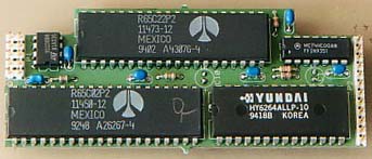
I'm using the watchdog timer's socket as the "expansion port." Unfortunately, the highest address line present at that socket is A4. A12 is available at the EPROM socket, but not RWB. RAM is soldered to the board, and is an SOJ32 package, so that isn't a good access point either. I don't know that I have a practical way to load all 16 address lines.

Quote:
There have been times in the past that I have been pleasantly surprised to hear of people doing what the data sheets imply is impossible.

It's fairly typical in electronics that published maximum ratings tend to be conservative. In high volume production, you have to spec your product so reject rates are kept reasonably low. You recall in the early days of semiconductor production when manufacturers saw 40 to 50 percent good yield as excellent. That had quite a bit to do with what complex semiconductors like microprocessors cost back then. The yields have improved quite a bit since then, but much of that was a better way of rating parts so the majority of them would meet specs. That inevitably meant many would exceed specs.

The only thing is it's risky to base a design on an implied capability. The two TTL rating of the 65C22 is probably quite conservative, but would be expected to be conservative when one considers the volume of those things that gets made each year. It could be the 'C22 can drive 10 TTL loads. However, I don't think it could be expected in every case. I'm sure we can bet that there are going to be marginal examples now and then.

When I get around to building POC V2 I will have a fair amount invested in the project. In anticipation of building this more complicated (and more capable) device, I've upgraded my test bench setup (got a nifty refurbished HP 1725A 'scope with a 275 MHz rating, plus new probes) and gotten some other gear to facilitate the inevitable hardware debugging. While I'm always prepared for the possibility that it just flat won't work, more like it will be a case of "it sort of works," just like POC V1 did when I first got it going. Hence I'm being careful of not pushing things to a point where failure is likely. That means carefully anticipating the bus drive requirements so the thing doesn't fall on its face at anything higher than one or two MHz. :lol:

Quote:
To find the point of maximum performance, I had even thought of trying to adjust the clock input duty cycle in case symmetrical is not quite ideal, and using an adjustable delay line for the '573 address-high latch enable, to go from a little ahead of the system Ф2 to a little behind it, keep adjusting, and check the frequency where it starts to have problems, adjust, check, adjust, check, until I'm satisfied I can't get any more out of it.

I'm not likely to ever try anything like that, simply because using a CPLD solves the propagation time issues, as well as the complex logic functions. I did work out timing at one time using 74ABT logic to drive the address and data lines, and concluded that memory logic timing violations would occur at about 15 MHz (the problem comes from the cascading of the bus drivers' prop delay with the memory decoding logic's prop delay). I've opined before that it can't be done at 20 MHz with discrete gates, and still believe that to be the case. In any case, a CPLD makes things quite a bit easier.

The Atmel AT1508AS CPLD I'm looking at is available in speed grades to 7.5ns, which is more than adequate for meeting all setup requirements with a 20 MHz Ø2 clock (actually, the 10ns part is fine). Since the AT1508AS can source or sink 35 mA per output (Xilinx has similar ratings for their 95xx parts) I'm also anticipating bus drive strength will not be a problem in those circuits controlled by the CPLD. All data lines will be through the CPLD in the linear memory model, since they can (should) be isolated from the MPU during Ø2 low, leaving only the A16-A23 lines "hot" during that part of the bus cycle. So the CPLD can act as a line driver, as well as a logic device. If I choose the segmented memory model, D0-D7 will not be through the CPLD, which means I might be forced to use discrete line drivers.

Not all MPU address lines would be connected to the CPLD (I'm not anticipating the need to decode memory all the way down to A0), so I may have a situation where some address lines, most likely A0-A7, would be connected directly from the MPU to system hardware. That's the bus loading about which I'm concerned. It also gives rise to a potential issue involving slew.

If A0-A7 are directly connected to RAM, ROM and I/O hardware, the hardware will see a change of state on those address lines before a similar change would appear on A8-A23, due to propagation time in the CPLD. I don't know that such slew will pose a problem, since there would be adequate time during the low half of Ø2 (25ns at 20 MHz) for the CPLD to work its magic, and in any case, no chip will be paying attention to what the address bus is doing until a chip select has been asserted. So the slew issue may be a non-issue.

In summary, there are few unknowns that can't be answered with implied capabilities. I'm inclined to think that using line drivers of some sort would be the safe route in assuring that bus loading won't sabotage timing as the clock gets bumped up. But I'm still mulling this over.

_________________
x86?  We ain't got no x86.  We don't NEED no stinking x86!


Last edited by BigDumbDinosaur on Sun May 06, 2012 5:48 pm, edited 1 time in total.

Top
 Profile  
Reply with quote  
PostPosted: Sun May 06, 2012 10:12 am 
Offline
User avatar

Joined: Thu Dec 11, 2008 1:28 pm
Posts: 10798
Location: England
Hi BDD
could you say anything about the difference between driving TTL-style loads and CMOS-style loads? In my understanding, they are quite different - the difference between a transistor's emitter terminal and a capacitor. This is why it is (or was) hard to drive a lot of TTL loads, and why the specified capability is so poor. But surely most chips these days - certainly your chosen SRAMs, and the CPU - present a CMOS load, which is purely capacitative. If I understand correctly, the available drive from an output used to be a matter of pass/fail (as TTL load increases) and now becomes a matter of maximum speed (as CMOS load increases). So fanout capability used to be a hard limit, but now we have a speed limit.

Or, is it the case that you still have some genuine TTL-style loads on the bus?

Cheers
Ed


Top
 Profile  
Reply with quote  
PostPosted: Sun May 06, 2012 7:00 pm 
Offline
User avatar

Joined: Thu May 28, 2009 9:46 pm
Posts: 8175
Location: Midwestern USA
BigEd wrote:
Hi BDD
could you say anything about the difference between driving TTL-style loads and CMOS-style loads? In my understanding, they are quite different - the difference between a transistor's emitter terminal and a capacitor. This is why it is (or was) hard to drive a lot of TTL loads, and why the specified capability is so poor. But surely most chips these days - certainly your chosen SRAMs, and the CPU - present a CMOS load, which is purely capacitative. If I understand correctly, the available drive from an output used to be a matter of pass/fail (as TTL load increases) and now becomes a matter of maximum speed (as CMOS load increases). So fanout capability used to be a hard limit, but now we have a speed limit.

Or, is it the case that you still have some genuine TTL-style loads on the bus?

Cheers
Ed

I'm using 100 percent CMOS—no TTL loads. However, while the static input current to a CMOS device is very low (a few microamps in some cases), current is required to charge those CMOS "capacitors," which charging current, of course, would have to be provided by the device driving the line(s). Since the drive source has some internal resistance, in effect, each line has an RC time constant that has to be accounted for in determining the highest rate at which the system can run. Quantifying that time constant is not easy—some of it gets into the realm of transmission line theory, which is definitely not an area of expertise for me (my knowledge in that arena stops in the mid-1960s with my electrical engineering education).

Since the R in the RC time constant will mostly be in the device driving the line, it can be *roughly* estimated by using the maximum sinking or sourcing current rating and the output voltage in each logic state. It stands to reason that the time constant can be reduced if the driving device has high drive strength, since that implies low R. Much of the C can be determined by summing the input capacitance ratings of the devices at the other end of the line. However, the board itself contributes capacitance that is difficult to estimate. There are a number of variables that get into the picture, such as trace routing, the number of layers, use of filled planes (not a good idea in high speed digital work), the dielectric constant of the board material, etc. Even the thickness of the solder mask coating can affect distributed capacitance.

My point to this diatribe is if the capacitive loading cannot be adequately defined, then the only recourse is probably to use line drivers (the 74ABT types, which can source at least 64 mA, but introduce only a few ns delay) between the MPU and the loads. I'm not as confident of the '816's drive strength as Garth is, although I do acknowledge to his greater experience with that sort of thing. Assuming the '816 has the same drive strength as the 65C22, two TTL loads, that's only about 3 mA that can be counted on. While that would have no problem driving a bunch of CMOS devices, the effective series resistance in the '816 would be an adverse factor in determining the RC time constant of the circuit, placing a hard limit on maximum system speed. It all comes back to how much silicon I will be attaching to the buses. As I earlier said, a maximum amount of RAM would entail the use of 32 SRAMs, each with an average input capacitance of 8 pF (for Cypress CY7C1049D SRAMs, like those used by Garth on his DIMM).

If I do use line drivers, I would be using SOIC packages, which don't consume a lot of board real estate. The smaller package itself will introduce less capacitance. So it may prove to be a worthwhile design choice.

_________________
x86?  We ain't got no x86.  We don't NEED no stinking x86!


Top
 Profile  
Reply with quote  
PostPosted: Sun May 06, 2012 7:11 pm 
Offline
User avatar

Joined: Thu Dec 11, 2008 1:28 pm
Posts: 10798
Location: England
The datasheet suggests timings are taken at 35pF loading - as you say, external R and C from the board is a variable. Naively one might try to drive 4 SRAMs direct from the CPU but not 32.
Cheers
Ed


Top
 Profile  
Reply with quote  
PostPosted: Mon May 07, 2012 2:04 am 
Offline
User avatar

Joined: Fri Aug 30, 2002 1:09 am
Posts: 8432
Location: Southern California
Quote:
However, the board itself contributes capacitance that is difficult to estimate.

It's not difficult to measure though. :wink: I just measured from one of the traces on the memory module that runs along a wide ground trace, to both power and ground combined, and got 4pF. I tried to pick the worst one. Next I measured a pin header and socket combination, one pin to the five pins around it combined (those other five connected together for the test) and got 2pF. The resolution on the meter is 1pF and the reading was vacillating between 1 and 2pF but spending more time at 2pF. The conclusion is that the board itself, including the in header and socket, will have very little capacitance compared to the ICs on it. Granted, it's not a multi-layer board.

Edit: Next, on this multilayer board I've shown before
Image
(which has the ROM on the other side), I measured the capacitance of the longest .007"-wide trace on a layer that's only separated from a plane layer by about .005-.006", and got 14pF. There's yet another advantage of using small SMT parts and getting them close together and keeping the board small: the shorter traces lets you can minimize the capacitance between traces and the planes. This is ridiculous though. I filed into the edge to get to pads along the edge to see the layer spacing under the microscope. I did not specify to the manufacturer how the six layers should be spaced, and they sure didn't space them evenly. From this layer to the next layer on the other side was 2-3 times as far as to the nearby plane layer.

Quote:
There are a number of variables that get into the picture [...] the dielectric constant of the board material

That's 4.1 for the standard FR-4 board material.

_________________
http://WilsonMinesCo.com/ lots of 6502 resources
The "second front page" is http://wilsonminesco.com/links.html .
What's an additional VIA among friends, anyhow?


Top
 Profile  
Reply with quote  
PostPosted: Mon May 07, 2012 5:36 pm 
Offline
User avatar

Joined: Thu May 28, 2009 9:46 pm
Posts: 8175
Location: Midwestern USA
GARTHWILSON wrote:
Quote:
There are a number of variables that get into the picture [...] the dielectric constant of the board material

That's 4.1 for the standard FR-4 board material.

I couldn't recall the number. Too many numbers and not enough synapses. :D

_________________
x86?  We ain't got no x86.  We don't NEED no stinking x86!


Top
 Profile  
Reply with quote  
Display posts from previous:  Sort by  
Post new topic Reply to topic  [ 8 posts ] 

All times are UTC


Who is online

Users browsing this forum: No registered users and 8 guests


You cannot post new topics in this forum
You cannot reply to topics in this forum
You cannot edit your posts in this forum
You cannot delete your posts in this forum
You cannot post attachments in this forum

Search for:
Jump to: