ElEctric_EyE wrote:
This is an ingenious idea though, putting the cap into a via. Only potential problem is putting too much solder into the via, but as Garth noted, check for a short circuit after soldering each and every cap.
You could probably do the same thing with a pad, which unlike a via, is not ephemeral.
Quote:
This recent discussion has reminded me to keep distances short when planning traces for bypass caps in my project, something I've not strictly adhered to in my recent designs. I had forgotten the importance of it...
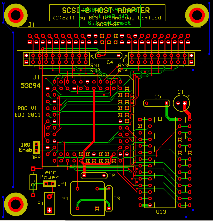
Yes. Short and thick. In my designs, I tend to connect the "positive" side of the decoupling cap to Vcc (this is usually on a 4-layer board) and connect the Vcc pin(s) of the chip to the cap using a thick trace, not the power plane/layer. Hence the only path for switching noise is back to the decoupling cap, helping to minimize propagation to other board areas via the power plane/layer. If possible, I also connect the ground pin(s) of the chip to the ground side of the cap in the same fashion. I did this on my
new SCSI host adapter. The 53C94 controller makes quite a bit of (electronic) racket, thanks, in part, to the 48 ma active outputs on all 18 SCSI pins. None of it is showing up in the power and ground layers.
Quote:
I would've liked to use this concept though I don't think I can take advantage of it on a 4 layer board, with the internal 2 layers being GND and Power.
Probably not. Drilling out the plate-through in a via or pad connected to one of the inner layers would most likely break the connection. Plus you'd run the risk of shorting the inner layers together and converting the PCB into a nice (and expensive) bookmark.


