bogrol wrote:
The rest of it is the same as the simplified version of Garth's schematics by Ben Eater, the VIA is mapped by A13.
I'm not familiar with this, so a link to Ben's version would be helpful. And indeed, I suggest you make a schematic diagram
of your own version... of Ben's version of Garth's version!

Seriously, I recommend you have an actual diagram of your own project. That's because it will end up being unique (what with the 8250 and other details). It's much less error-prone to have all the information in one place (as compared with looking at someone else's diagram, while meanwhile trying to remember how you own version differs).
Quote:
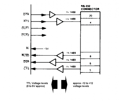
On the datasheet scheme you linked, are the triangles to the right also NOTs?
No, those are sections of a 1488 IC and sections of a 1489 IC. Their job is to convert the voltage levels of incoming and outgoing signals, because it's sometimes the case that you'll want +/- 12V levels... or not, depending on what sort of device attaches to the other end of your serial connection. BTW, modern equivalent ICs are preferable in some ways to the venerable 1488 and 1489.
Attachment:
 voltage levels.png [ 39.9 KiB | Viewed 2432 times ]
bogrol wrote:
bogrol wrote:
- WR active low (pin 18) to 5V, active high (pin 19) to R/W
- RD active low (pin 21) to R/W, active high (pin 22) to GND
The R/W signal I'm referring to is the one directly from the 6502.
This won't work, I'm afraid. And BTW trying to EXPLAIN connections can get quite confusing.

A diagram (as I suggested) is much better.
Quote:
Ps. I'm out of board space for a port built with discrete parts as suggested by plasmo.
Hmm, but didn't you mention a VIA?

You could use one of the VIA's ports for plasmo's suggestion...
-- Jeff
_________________
In 1988 my 65C02 got six new registers and 44 new full-speed instructions!
https://laughtonelectronics.com/Arcana/ ... mmary.html


