digidice wrote:
Been Enjoying the list now for a few months and have always wanted to basically roll my own ever since I seen PE come out with the ELF project of yesteryear. So I have been looking at schematics and decided I might toy with the idea of making my own C64 ish flavor of computer.
Okay so before you laugh, Its really an attempt to understand basic computer arch as well as machine code which would come next.
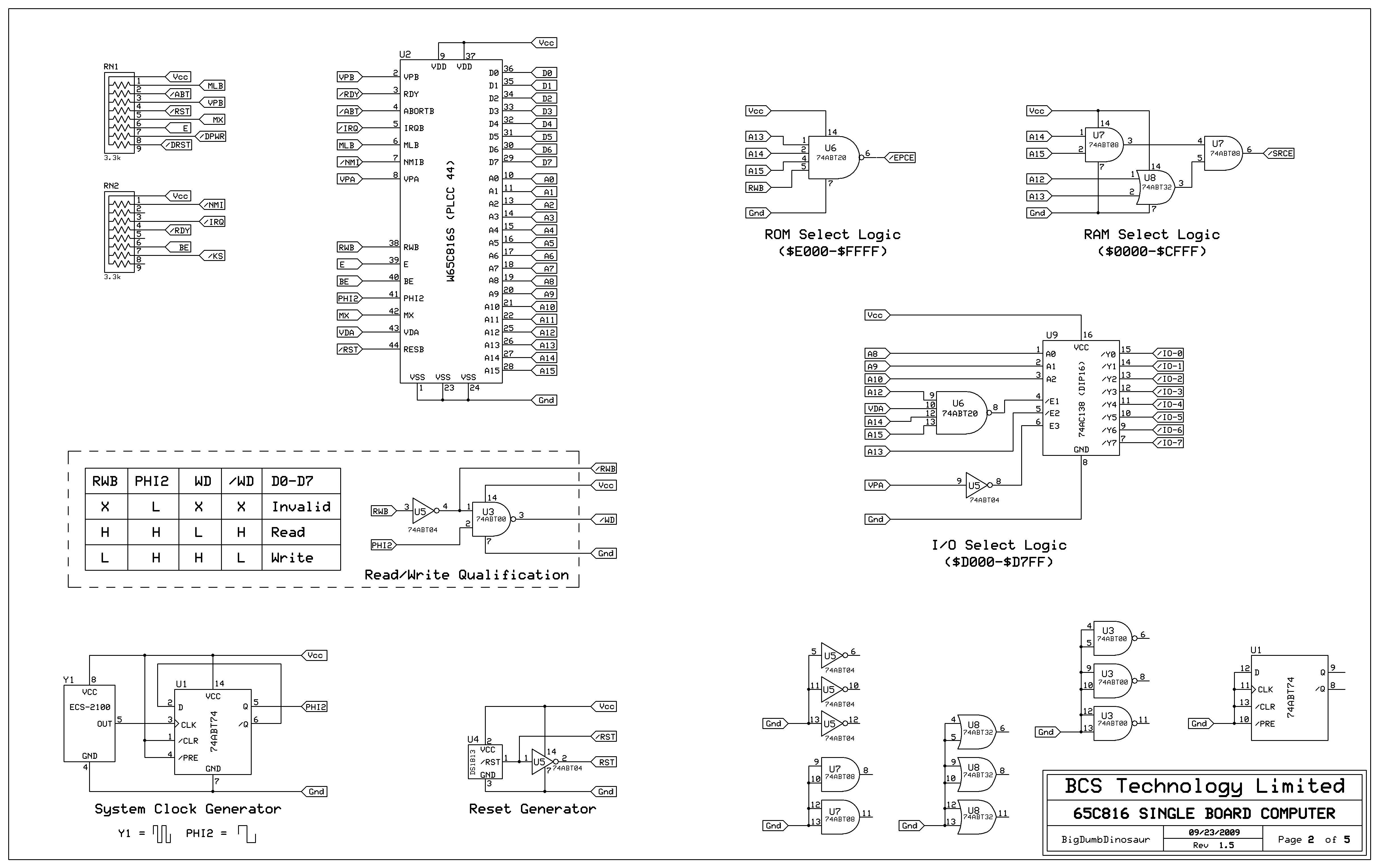
Now I know the original used a Programmable logic array (U8), but I want to try to keep away from that for the time being. So may I present to you something that I threw together tonight in an attempt to come to grips with how to pull a CE line from the address bus, now Im sure there is other chips I could have selected and wired them up differently and all comments are welcome. Is this on the right track? or is this not how it would be done with discrete devices?
Simple SchematicA couple of thoughts:
1) As suggested by Ruud, decoding with a 74*138 would make for a lower parts count and a less difficult to debug design. Your address decoding is going to suffer significant prop delays with all those gates. Be that as it may, I'm sure it'll run at least as fast as the real C-64.

2) Your design doesn't account for the VDA and VPA signals emitted by the W65C816S. The '816 generates spurious bus accesses during the intermediate stages of executing some instructions. VDA and VPA have been provided to identify and avoid such conditions. Failing to account for those two signals may lead to obdurate bus issues.
3) The '816 is a CMOS device and should used with CMOS glue logic where possible. With the exception of the 4000 series logic (which, as Garth noted, is dog-slow and should not be used), everything can be implemented in 74ABT or 74AC logic, which are substantially faster than 74LS logic.
Quote:
In retrospect the 300ns is too long because I really want to run this thing at close the 14Mhz, IE some 20ns good up to 50Mhz. which is also the reason I dont want to use an eprom or the PAL that came with the C-64...
4) You'll be struggling to get up to 14 MHz with this setup. I see 8 MHz as a stretch, given the circuit you have right now. At 14 MHz, machine cycle time is 70ns. Address setup has to be completed by the rise of Ø2, which means you'd only have about 25ns max for address setup. My opinion is it isn't going to happen with all that discrete logic. Also, you may be faced with wait-stating I/O accesses, depending on what you use for I/O hardware.
kc5tja wrote:
The C64 and C128 both depend on PALs (the C64 uses the 82S100, IIRC; not sure what the C128 uses).
The C-128 used both an MMU and PAL, the former being the device that worked out the mix of RAM, ROM and I/O. The details are no longer in my head, unfortunately (ain't aging a bitch?).


