6502.org Forum  Projects  Code  Documents  Tools  Forum
It is currently Sat Apr 20, 2024 2:50 am

All times are UTC


Post new topic Reply to topic  [ 544 posts ]  Go to page Previous  1 ... 12, 13, 14, 15, 16, 17, 18 ... 37  Next
Author Message
 Post subject: POC Version 2 Logic
PostPosted: Mon Nov 17, 2014 2:29 am 
Offline
User avatar

Joined: Thu May 28, 2009 9:46 pm
Posts: 8138
Location: Midwestern USA
This project is still languishing, as for some reason I can't seem to get my head around the CUPL code needed to program the CPLD. Adding to the fun, I discovered some irritating bugs in Atmel's WinCUPL that wasted a fair amount of my time as I tried to convert what I want the circuit to do into the mumbo-jumbo understood by the CUPL compiler. Some of the syntax described in the CUPL programming manual is either not correctly implemented in the compiler, or is not supported at all.

One thing that has become quite clear is that WinCUPL is not very good software. It is touchy about what's in the source code and will crash in some cases during compilation if an error is encountered. WinCUPL appears to have originally been an MS-DOS program that got "WIMPed" back in the days of Windows 95/98 and hasn't seen much maintenance since then. The latest date that I could find indicating that anyone had a look at the code is in 2004. Testing has determined that it is unstable on Windows 7 64 bit (which I don't use—I cannot stand its user interface). Oddly, running the UNIX strings command on the executable turns up references to Logical Devices Corp., the originators of CUPL. They haven't been around for years.

_________________
x86?  We ain't got no x86.  We don't NEED no stinking x86!


Top
 Profile  
Reply with quote  
 Post subject: Re: POC Version 2
PostPosted: Mon Nov 17, 2014 3:02 pm 
Offline

Joined: Mon Mar 02, 2009 7:27 pm
Posts: 3258
Location: NC, USA
Screw Atmel BDD. I never liked not being able to program their GAL22 IC because of their proprietary algorithm when I first got into programmable logic.
I know it's difficult sometimes to loose allegiance to a particular company, but Xilinx has some great software. Heck you can even choose schematic entry for your CPLD.
But maybe the issue is 5v compatibility?

_________________
65Org16:https://github.com/ElEctric-EyE/verilog-6502


Top
 Profile  
Reply with quote  
 Post subject: Re: POC Version 2
PostPosted: Mon Nov 17, 2014 4:44 pm 
Offline
User avatar

Joined: Thu May 28, 2009 9:46 pm
Posts: 8138
Location: Midwestern USA
ElEctric_EyE wrote:
Screw Atmel BDD. I never liked not being able to program their GAL22 IC because of their proprietary algorithm when I first got into programmable logic.
I know it's difficult sometimes to loose allegiance to a particular company, but Xilinx has some great software. Heck you can even choose schematic entry for your CPLD.
But maybe the issue is 5v compatibility?

The issue is 5 volt compatibility. Only Atmel and Altera continue to produce 5 volt CPLDs. Switching to Altera would be a PITA for several reasons.

_________________
x86?  We ain't got no x86.  We don't NEED no stinking x86!


Top
 Profile  
Reply with quote  
 Post subject: Re: POC Version 2
PostPosted: Mon Nov 17, 2014 5:15 pm 
Offline
User avatar

Joined: Tue Mar 02, 2004 8:55 am
Posts: 996
Location: Berkshire, UK
I run WinCUPL on an old XP laptop which solves some of the stability issues but I still always save before compiling and make frequent backups.

You could probably achieve the same thing running XP in a virtual machine under either Windows 7 or Linux. I use VirtualBox to create expendable XP development environments on my main Windows 7 64-bit machine for legacy software like this.

_________________
Andrew Jacobs
6502 & PIC Stuff - http://www.obelisk.me.uk/
Cross-Platform 6502/65C02/65816 Macro Assembler - http://www.obelisk.me.uk/dev65/
Open Source Projects - https://github.com/andrew-jacobs


Top
 Profile  
Reply with quote  
 Post subject: Re: POC Version 2
PostPosted: Mon Nov 17, 2014 5:33 pm 
Offline
User avatar

Joined: Thu May 28, 2009 9:46 pm
Posts: 8138
Location: Midwestern USA
BitWise wrote:
I run WinCUPL on an old XP laptop which solves some of the stability issues but I still always save before compiling and make frequent backups.

You could probably achieve the same thing running XP in a virtual machine under either Windows 7 or Linux. I use VirtualBox to create expendable XP development environments on my main Windows 7 64-bit machine for legacy software like this.

I have one XP box here, which is where I run WinCUPL. I had the same problems with WinCUPL when I was running Windows 2000, so it's more likely just buggy software and not anything specific to the operating system. Atmel really needs to give that software a refresh. The documentation is also horribly out of date. Why sell a product if you're not going to adequately support it?

_________________
x86?  We ain't got no x86.  We don't NEED no stinking x86!


Top
 Profile  
Reply with quote  
 Post subject: Re: POC Version 2
PostPosted: Mon Nov 17, 2014 8:29 pm 
Offline

Joined: Mon Aug 05, 2013 10:43 pm
Posts: 258
Location: Southampton, UK
ElEctric_EyE wrote:
...but Xilinx has some great software. Heck you can even choose schematic entry for your CPLD. But maybe the issue is 5v compatibility?


I've not used Atmel's tools, but I have used Xilnix's and they are certainly decent.

Though they are no longer made, the XC9500s are excellent parts IMO. AFAIK the largest one made in 5V was the 108, in PLCC84. Yes, they are discontinued, but they are not that difficult to find, and still supported by the Xilinx tools.

_________________
8 bit fun and games: https://www.aslak.net/


Top
 Profile  
Reply with quote  
 Post subject: Re: POC Version 2 Logic
PostPosted: Sun Nov 30, 2014 10:12 pm 
Offline
User avatar

Joined: Thu May 28, 2009 9:46 pm
Posts: 8138
Location: Midwestern USA
BigDumbDinosaur wrote:
...Adding to the fun, I discovered some irritating bugs in Atmel's WinCUPL that wasted a fair amount of my time as I tried to convert what I want the circuit to do into the mumbo-jumbo understood by the CUPL compiler. Some of the syntax described in the CUPL programming manual is either not correctly implemented in the compiler, or is not supported at all.

I did get some help on this from Atmel and learned that some bugs are well-known. The question is why haven't they been resolved?

Anyhow, I was able to build and compile CUPL code for the ATF1508AS CPLD. Here's what I've developed so far:

Code:
/*
* * * * * * * * * * * * * * * * * * * * * * * * * * * * * * * * * * * * * * * * * *
*                                                                                 *
*                 W65C816S PROOF OF CONCEPT SINGLE-BOARD COMPUTER                 *
*                                                                                 *
* =============================================================================== *
*                                                                                 *
*     Copyright (c)1991-2014 by BCS Technology Limited.  All rights reserved.     *
*                                                                                 *
* Permission is hereby granted to use, copy, modify and distribute this software, *
* provided this copyright notice remains unaltered in the source code and  proper *
* attribution is given.  Redistribution, in any form, must be at no charge to the *
* end user.  This code or any part  thereof, including any derivation, MAY NOT be *
* incorporated into any package intended for sale unless written permission to do *
* so has been granted by the copyright holder.                                    *
* ------------------------------------------------------------------------------- *
* THERE IS NO WARRANTY OF ANY KIND WITH THIS SOFTWARE.                            *
*                                                                                 *
* While it is believed that all code will perform as intended,  the user  assumes *
* all risk in connection with the incorporation of this software into any system. *
*                                                                                 *
* * * * * * * * * * * * * * * * * * * * * * * * * * * * * * * * * * * * * * * * * *

* * * * * * * * * *
* VERSION HISTORY *
* * * * * * * * * *

Ver    Rev Date    Revision
--------------------------------------------------------------------------------
0.1.0  2014/02/17  Original version.
0.2.0  2014/07/21  Added wait-state logic
0.3.0  2014/09/07  Added hardware management unit (HMU).
0.4.0  2014/10/18  Added "bleed-through" to write accesses to ROM.
0.5.0  2014/11/24  Added ability to map out ROM and/or I/O to expose RAM at same
                   address.  Change doesn't affect HMU,
0.5.1  2014/11/25  Some intermediate logic defintions changed to pinnodes to re-
                   duce number of product terms on some outputs.
--------------------------------------------------------------------------------
*/

Name        glue;
PartNo      B402170001;
Date        2014/02/17;
Revision    0.5.0;
Designer    BDD;
Company     BCS Technology Limited;
Assembly    POC V2;
Location    U2;
Device      f1508plcc84;

/*
===============================================================================

                          ATF1508AS (PLCC-84)
                 ______________________________________
                |                                      |
       RESB x---|1 INPUT/GCLR              INPUT/OE1 84|---x
            x---|2 INPUT/OE2/GCLK2       INPUT/GCLK1 83|---x CLKP
        Vcc x---|3 VccINT                        Gnd 82|---x Gnd
       ABTB x---|4 I/O                      IO/GCLK3 81|---x E
       IRQB x---|5 I/O                           I/O 80|---x RWB
         A0 x---|6 I/O                           I/O 79|---x VDA
        GND x---|7 Gnd                         VccIO 78|---x Vcc
        VPB x---|8 I/O                           I/O 77|---x RDY
        VPA x---|9 I/O                           I/O 76|---x A15
         A1 x---|10 I/O                          I/O 75|---x A14
       NMIB x---|11 I/O                          I/O 74|---x D7
            x---|12 IO/PD                        I/O 73|---x D4
        Vcc x---|13 VccIO                        Gnd 72|---x Gnd
            x---|14 IO/TDI (JTAG)      IO/TDO (JTAG) 71|---x
         A2 x---|15 I/O                          I/O 70|---x D5
            x---|16 I/O                          I/O 69|---x A18
            x---|17 I/O                          I/O 68|---x A17
            x---|18 I/O                          I/O 67|---x A16
        Gnd x---|19 Gnd                        VccIO 66|---x Vcc
            x---|20 I/O                          I/O 65|---x /RD
            x---|21 I/O                          I/O 64|---x D0
            x---|22 I/O                          I/O 63|---x D6
            x---|23 IO/TMS (JTAG)      IO/TCK (JTAG) 62|---x
       /EWS x---|24 I/O                          I/O 61|---x D1
            x---|25 I/O                          I/O 60|---x D2
        Vcc x---|26 VccIO                        Gnd 59|---x Gnd
            x---|27 I/O                          I/O 58|---x D3
        RST x---|28 I/O                          I/O 57|---x /RAM
            x---|29 I/O                          I/O 56|---x /WD
            x---|30 I/O                          I/O 55|---x /ROM
            x---|31 I/O                          I/O 54|---x A13
        Gnd x---|32 Gnd                        VccIO 53|---x Vcc
            x---|33 I/O                          I/O 52|---x A11
            x---|34 I/O                          I/O 51|---x A12
            x---|35 I/O                          I/O 50|---x A10
            x---|36 I/O                          I/O 49|---x A8
       /IO2 x---|37 I/O                          I/O 48|---x A9
        Vcc x---|38 VccIO                        Gnd 47|---x Gnd
       /IO3 x---|39 I/O                          I/O 46|---x /IO1
            x---|40 I/O                        IO/PD 45|---x
       /IO0 x---|41 I/O                          I/O 44|---x /IO4
        Gnd x---|42 Gnd                       VccINT 43|---x Vcc
                |______________________________________|
*/

/*
=====================
INPUT PIN ASSIGNMENTS
=====================
*/
pin       = A0;                                   /* address line $000001          */
pin       = A1;                                   /* address line $000002          */
pin       = A2;                                   /* address line $000004          */
pin       = A8;                                   /* address line $000100          */
pin       = A9;                                   /* address line $000200          */
pin       = A10;                                  /* address line $000400          */
pin       = A11;                                  /* address line $000800          */
pin       = A12;                                  /* address line $001000          */
pin       = A13;                                  /* address line $002000          */
pin       = A14;                                  /* address line $004000          */
pin       = A15;                                  /* address line $008000          */
pin    24 = !EWS;                                 /* enable wait-stating           */
pin       = IRQB;                                 /* MPU maskable interrupt        */
pin       = NMIB;                                 /* MPU nonmaskable input         */
pin       = E;                                    /* MPU operating mode            */
pin       = RWB;                                  /* MPU read/write                */
pin       = VDA;                                  /* MPU valid data address        */
pin       = VPA;                                  /* MPU valid instruction address */
pin       = VPB;                                  /* MPU interrupt vector pull     */
pin    83 = PHI2;                                 /* system clock                  */
pin     1 = RESB;                                 /* system reset                  */

/*
======================
OUTPUT PIN ASSIGNMENTS
======================
*/
pin       = A16;                                  /* address line $010000  */
pin       = A17;                                  /* address line $020000  */
pin       = A18;                                  /* address line $040000  */
pin       = ABTB;                                 /* MPU abort interrupt   */
pin       = !IO0;                                 /* I/O device 'A' select */
pin       = !IO1;                                 /* I/O device 'B' select */
pin       = !IO2;                                 /* I/O device 'C' select */
pin       = !IO3;                                 /* I/O device 'D' select */
pin       = !IO4;                                 /* I/O device 'E' select */
pin       = !RST;                                 /* inverted reset        */
pin       = !RAM;                                 /* RAM chip select       */
pin       = !RD;                                  /* read data             */
pin       = !ROM;                                 /* ROM chip select       */
pin       = !WD;                                  /* write data            */

/*
=============================
BIDIRECTIONAL PIN ASSIGNMENTS
=============================
*/
pin       = D0;                                   /* data line $01 */
pin       = D1;                                   /* data line $02 */
pin       = D2;                                   /* data line $04 */
pin       = D3;                                   /* data line $08 */
pin       = D4;                                   /* data line $10 */
pin       = D5;                                   /* data line $20 */
pin       = D6;                                   /* data line $40 */
pin       = D7;                                   /* data line $80 */
pin       = RDY;                                  /* MPU wait      */

/*
==========================================================
MACHINE ARCHITECTURE & HARDWARE MANAGEMENT UNIT DEFINTIONS
==========================================================

           +--------------------------+ $07FFFF
           |                          |
           |       RAM (448 KB)       |
           |                          |
   +-------+--------------------------+ $010000
   |       |                          |
   | E-RAM |       E-ROM (8 KB)       |
   |       |                          |
   +-------+--------------------------+ $00E000
           | Hardware Management Unit |
   +-------+--------------------------+ $00DF00
   |       |                          |
   | D-RAM |       I/O (3.75 KB)      |
   |       |                          |
   +-------+--------------------------+ $00D000
   |       |                          |
   | C-ROM |       C-RAM (4 KB)       |
   |       |                          |
   +-------+--------------------------+ $00C000
           |                          |
           |       RAM (48 KB)        |
           |                          |
           +--------------------------+ $000000

                1 KB = 1024 bytes

  HMU               
Register   Address   Register Description    Bit  Function                        Notes
---------------------------------------------------------------------------------------
hmumcfg    $00DF00   System configuration:    0   0: C-RAM write-protection off     A
                                                  1: C-RAM write-protection on
                                              1   0: E-RAM write-protection off     A
                                                  1: E-RAM write-protection on
                                              2   not defined
                                              3   0: I/O                            A
                                                  1: D-RAM
                                              4   0: C-RAM                          A
                                                  1: C-ROM
                                              5   0: E-ROM                          A
                                                  1: E-RAM
                                              6   0: bank $00 remapping off         A
                                                  1: bank $00 remapping on
                                              7   0: hardware protection off       A,B
                                                  1: hardware protection on

hmubnki    $00DF01   In-context bank
hmubnks    $00DF02   System mode bank
hmubnku    $00DF03   User mode bank
hmupisr    $00DF04   Interrupt status:       0-2  interrupting device ID           C,D
                                              6   1: NMI detected
                                              7   1: IRQ detected

hmupimr    $00DF05   Interrupt masks:         0   1: IRQ A enabled
                                              1   1: IRQ B enabled
                                              2   1: IRQ C enabled
                                              3   1: IRQ D enabled

hmustat    $00DF06   System status:           6   0: supervisor mode enabled       A,C
                                                  1: user mode enabled
                                              7   1: SCSI DMA request active
----------------------------------------------------------------------------------------
Notes: A) Default following reset.
       B) Also disables bank $00 remapping.
       C) Read only register.
       D) Valid only if bit 7 = 1.
*/

$DEFINE   cblkwpe   hmumcfg0
$DEFINE   eblkwpe   hmumcfg1
$DEFINE   dblkmap   hmumcfg3
$DEFINE   cblkmap   hmumcfg4
$DEFINE   eblkmap   hmumcfg5
$DEFINE   bnk0rmap  hmumcfg6
$DEFINE   protect   hmumcfg7

$DEFINE   activirq  [hmupisr0..2]
$DEFINE   nmimask   hmupisr6
$DEFINE   irqmask   hmupisr7

$DEFINE   irqaenab  hmupimr0
$DEFINE   irqbenab  hmupimr1
$DEFINE   irqcenab  hmupimr2
$DEFINE   irqdenab  hmupimr3

$DEFINE   protmode  hmustat6
$DEFINE   scsidreq  hmustat7

/*
=========================
BURIED LOGIC DECLARATIONS
=========================
*/
node        bank0;                                /* 1 = $000000-$00FFFF being accessed   */
pinnode   = [blatch0..2];                         /* A16-A18 latches                      */
node        dblk;                                 /* 1 = $00D000-$00DFFF being accessed   */
pinnode   = [hmubnki0..7];                        /* HMU in-context bank register         */
pinnode   = [hmubnks0..7];                        /* HMU supervisor mode bank register    */
pinnode   = [hmubnku0..7];                        /* HMU user mode bank register          */
pinnode   = [hmumcfg0..7];                        /* HMU system configuration register    */
pinnode   = [hmupimr0..7];                        /* HMU interrupt mask register          */
/* pinnode   = [hmupisr0..7];                        /* HMU interrupt status register        */
pinnode   = [hmustat0..7];                        /* HMU system status register           */
node        hmurd;                                /* 1 = reading from HMU                 */
node        hmusel;                               /* 1 = HMU being accessed               */
node        hmuwd;                                /* 1 = writing to HMU                   */
node        ioblk;                                /* 1 = I/O address space being accessed */
node        iosel;                                /* 1 = I/O device being accessed        */
/* pinnode   = [irqn0..2];                           /* IRQ priority encoder bits            */
node        opcode;                               /* 1 = opcode fetch in progress         */
node        rdflag;                               /* 1 = data fetch in progress           */
node        rdyout;                               /* 1 = MPU wait-stated                  */
node        vbus;                                 /* 1 = address bus valid                */
node        vdbus;                                /* 1 = data address valid               */
node        vpbus;                                /* 1 = operand address valid            */
node        wdflag;                               /* 1 = data store in progress           */
node        wsenab;                               /* 1 = wait-state in progress           */
pinnode   = wsff;                                 /* wait-state flip-flop                 */

/*
=========================
REGISTER RESETS & PRESETS
=========================
*/
/* hmurd.AR         = !RESB;
hmusel.AR        = !RESB;
hmuwd.AR         = !RESB;
rdflag.AR        = !RESB;
rdyout.AR        = !RESB;
wdflag.AR        = !RESB;
wsenab.AR        = !RESB; */
wsff.AR          = !RESB;
/* hmurd.AP         = 'b'0;
hmusel.AP        = 'b'0;
hmuwd.AP         = 'b'0;
rdflag.AP        = 'b'0;
rdyout.AP        = 'b'0;
wdflag.AP        = 'b'0;
wsenab.AP        = 'b'0; */
wsff.AP          = 'b'0;
[hmumcfg0..7].AR = !RESB;
[hmubnki0..7].AR = !RESB;
[hmubnks0..7].AR = !RESB;
[hmubnku0..7].AR = !RESB;
/* [hmupisr0..7].AR = !RESB; */
[hmupimr0..7].AR = !RESB;
[hmustat0..7].AR = !RESB;
[hmumcfg0..7].AP = 'b'0;
[hmubnki0..7].AP = 'b'0;
[hmubnks0..7].AP = 'b'0;
[hmubnku0..7].AP = 'b'0;
/* [hmupisr0..7].AP = 'b'0; */
[hmupimr0..7].AP = 'b'0;
[hmustat0..7].AP = 'b'0;

/*
=================
BUS CONTROL LOGIC
=================
*/
opcode    =  VDA &  VPA;                          /* true if opcode fetch          */
vdbus     =  VDA & !VPA;                          /* true if valid data address    */
vpbus     = !VDA &  VPA;                          /* true if valid operand address */
vbus      =  VDA #  VPA;                          /* true if valid address         */
rdflag    = RWB & vbus;                           /* true if fetch operation       */
wdflag    = !RWB & vbus;                          /* true if store operation       */

/*
=========================
EXTENDED ADDRESSING LOGIC
=========================
*/
[blatch0..2].LE = vbus & !PHI2;
[blatch0..2].L  = vbus & !PHI2 & [D0..2];
bank0     = [blatch2..0]:'b'000;                  /* true if $000000-$00FFFF */
extram    = !bank0;                               /* true if $010000-$07FFFF */

/*
====================
MEMORY MAPPING LOGIC
====================
*/
basram    = (!A15 # !A14) & bank0;                /* $000000-$00BFFF */
cblk      = A15 & A14 & !(A13 # A12) & bank0;     /* $00C000-$00CFFF */
dblk      = A15 & A14 & !A13 & A12 & bank0;       /* $00D000-$00DFFF */
eblk      = A15 & A14 & A13 & bank0;              /* $00E000-$00FFFF */

ioblk     = dblk & !(A11 & A10 & A9 & A8);        /* I/O hardware    */

/* RAM selection rules... */

ramsel    = basram #                              /* base RAM     */
            cblk & (wdflag # !cblkmap) #          /* C-RAM        */
            ioblk & dblkmap #                     /* D-RAM        */
            eblk & (wdflag # eblkmap) #           /* E-RAM        */
            extram;                               /* extended RAM */

/* ROM selection rules... */

romsel    = cblk & rdflag & cblkmap #             /* C-ROM */
            eblk & rdflag & !eblkmap;             /* E-ROM */

/* I/O devices selection rules... */

iosel     = ioblk & !dblkmap;

/*
================
HMU ACCESS LOGIC
================
*/
hmusel    = dblk & A11 & A10 & A9 & A8;           /* HMU base selection        */
mcfgsel   = !A2 & !A1 & !A0;                      /* configuration register    */
ibnksel   = !A2 & !A1 &  A0;                      /* in-context bank register  */
sbnksel   = !A2 &  A1 & !A0;                      /* system mode bank register */
ubnksel   = !A2 &  A1 &  A0;                      /* user mode bank register   */
pisrsel   =  A2 & !A1 & !A0;                      /* IRQ status register       */
pimrsel   =  A2 & !A1 &  A0;                      /* IRQ mask register         */
statsel   =  A2 &  A1 & !A0;                      /* system status register    */
hmurd     = hmusel & rdflag & PHI2;               /* any register read         */
hmuwd     = hmusel & wdflag & PHI2;               /* any register write        */

/*
===========================
IRQ PRIORITY ENCODING LOGIC
===========================
*/
$IFDEF skip_this_code
table irqi => irqn {
  'b'xxxx1xxx => 'd'3;                            /* IRQ A */
  'b'xxxxx1xx => 'd'2;                            /* IRQ B */
  'b'xxxxxx1x => 'd'1;                            /* IRQ C */
  'b'xxxxxxx1 => 'd'0;                            /* IRQ D */
  'b'00000000 => 'd'0;                            /* no pending IRQ */
}
$ENDIF

/*
================
WAIT-STATE LOGIC
================

The following code causes a wait-state to occur on I/O or ROM accesses
if the EWS jumper block on the PCB is shorted.  A wait-state will last
for one phase-2 clock cycle.
*/
wsenab    = (iosel # romsel) & EWS;
wsff.CK   = PHI2 & wsenab;
wsff.D    = wsff & wsenab;
rdyout    = wsenab & wsff;

/*
=========================
CONTROL OUTPUT STATEMENTS
=========================
*/
[A16..18] = [blatch0..2] & vbus;                  /* A16-A18 address bits       */
ABTB      = 'b'1;                                 /* abort interrupt -- testing */
IO0       = iosel & !A10 & !A9 & !A8 & vbus;      /* I/O device 'A' select      */
IO1       = iosel & !A10 & !A9 &  A8 & vbus;      /* I/O device 'B' select      */
IO2       = iosel & !A10 &  A9 & !A8 & vbus;      /* I/O device 'C' select      */
IO3       = iosel & !A10 &  A9 &  A8 & vbus;      /* I/O device 'D' select      */
IO4       = iosel &  A10 & !A9 & !A8 & vbus;      /* I/O device 'E' select      */
RAM       = ramsel & vbus;                        /* RAM chip enable            */
RD        = (rdflag & PHI2 #
             rdflag & rdyout) & !hmusel;          /* active low read            */
RDY       = !rdyout;                              /* MPU wait-state input       */
RDY.oe    = wsenab;                               /* active if wait-stating     */
ROM       = romsel & vbus;                        /* ROM chip enable            */
RST       = RESB;                                 /* inverted reset             */
WD        = wdflag & (PHI2 # rdyout) & !hmusel;   /* active low write           */

/*
==============================
HMU REGISTER ACCESS STATEMENTS
==============================
*/

/* clocks... */

[hmumcfg0..7].CK = mcfgsel & hmuwd;
[hmubnki0..7].CK = ibnksel & hmuwd;
[hmubnks0..7].CK = sbnksel & hmuwd;
[hmubnku0..7].CK = ubnksel & hmuwd;
/* [hmupisr0..7].CK = pisrsel & hmuwd; */
[hmupimr0..7].CK = pimrsel & hmuwd;
[hmustat0..7].CK = statsel & hmuwd;

/* interrupt status conditioning... */

/* [hmupisr0..2].D  = !IRQB & 'b'1;                  /**** testing ****/
/* [hmupisr3..5].D  = 'b'1;                          /* unused ISR bits */
/* hmupisr{6}.D     = NMIB;                          /* nonmaskable interrupt */
/* hmupisr{7}.D     = IRQB;                          /* interrupt request     */

/* configuration & control register writes... */

[hmumcfg0..7].D  = mcfgsel & hmuwd & [D0..7];
[hmubnki0..7].D  = ibnksel & hmuwd & [D0..7];
[hmubnks0..7].D  = sbnksel & hmuwd & [D0..7];
[hmubnku0..7].D  = ubnksel & hmuwd & [D0..7];
[hmupimr0..7].D  = pimrsel & hmuwd & [D0..7];
[hmustat0..7].D  = statsel & hmuwd & [D0..7];

/* register reads... */

[D0..7].oe       = (
                    mcfgsel # ibnksel #
                    sbnksel # ubnksel #
                    pisrsel # pimrsel #
                    statsel
                   ) & hmurd;
[D0..7]          = (
                    mcfgsel & [hmumcfg0..7] #
                    ibnksel & [hmubnki0..7] #
                    sbnksel & [hmubnks0..7] #
                    ubnksel & [hmubnku0..7] #
                    /* pisrsel & [hmupisr0..7] # */
                    pimrsel & [hmupimr0..7] #
                    statsel & [hmustat0..7]
                   ) & hmurd;

/* * * * *  E N D   O F   F I L E  * * * * */

The above code incorporates some of the concepts I had worked on for a protected environment. It won't fit the 1508AS, however, without design changes to the board layout.

Attachment:
File comment: POC V2 w/ATF1508AS CPLD
pocv2pcb.gif
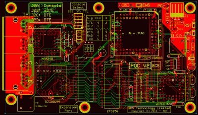
pocv2pcb.gif [ 112.84 KiB | Viewed 1167 times ]

A constraint of the EPCB Proto-Pro layout is the maximum allowable board size of 21 square inches (1354 square centimeters). The rectangular shape I conceived for POC V2 allows me to use the SCSI host adapter I devised for POC V1—the west end of the board has to stay unchanged so everything lines up. Unfortunately, that limits the space available to the CPLD and significantly limits the ability to use the topmost row of pins. However, the fitter that is part of Atmel's WinCUPL software can't fit my design to the 1508 as I want it. If I let the fitter auto-fit the design it works out fine, but results in many of the top row pins being assigned to a circuit function. I can move a few of the connections, but not enough to make it work.

It seems that I am going to be forced into using EPCB's production service so I can shape the PCB in a way that allows me to use the pins that are not readily accessible in the Proto-Pro layout. This issue is not unlike what ElEctric_EyE underwent in his project, except his problem was that of too many holes, rather than insufficient area. In my case, I'm okay with the hole count (637), but need more board area—my board is 6 inches × 3.5 inches, putting it right at the 21 square inch limit.

I'm going to work out a totally new board layout that is designed to make best use of the 1508, rather than work within the Proto-Pro limits, which should allow me to distribute I/O connections evenly around all sides of the device. I'm not seeing any other (obvious) solution.

_________________
x86?  We ain't got no x86.  We don't NEED no stinking x86!


Top
 Profile  
Reply with quote  
 Post subject: Re: POC Version 2
PostPosted: Mon Dec 01, 2014 1:13 am 
Offline
User avatar

Joined: Sun Jun 30, 2013 10:26 pm
Posts: 1922
Location: Sacramento, CA, USA
Those mounting holes @ 12:00 and 6:30 don't look necessary unless it's going to be used in a fighter jet, IMHO. Might you consider getting rid of them and doing a tiny bit of parts shuffling in order to get the space that you need at the top?

Mike


Top
 Profile  
Reply with quote  
 Post subject: Re: POC Version 2
PostPosted: Mon Dec 01, 2014 1:36 am 
Offline
User avatar

Joined: Thu May 28, 2009 9:46 pm
Posts: 8138
Location: Midwestern USA
barrym95838 wrote:
Those mounting holes @ 12:00 and 6:30 don't look necessary unless it's going to be used in a fighter jet, IMHO. Might you consider getting rid of them and doing a tiny bit of parts shuffling in order to get the space that you need at the top?

The hole at 12 o'clock is one of the three that secure the SCSI host adapter, so is necessary. I added the hole at 6:30 because flexing in that area would occasionally partially disengage the host adapter bus pins from the J5 socket into which it is plugged, this problem occurring with POC V1.1. Its removal would not really accomplish much, as the relationship between the holes at 10 o'clock, 12 o'clock and 8 o'clock and J5 socket must be maintained. Hence J5 can't be moved to occupy any of the space taken by the hole at 12:30.

The original plan for POC V2 was the use of the smaller Atmel 1504AS CPLD, which comes in a PLCC-44 package. My code fitted that device. Recall that the switch to the 1508AS was because I couldn't get my hands on the Atmel programmer adapter for the PLCC-44 package and couldn't program the device via JTAG, since those pins were being used as I/Os.

_________________
x86?  We ain't got no x86.  We don't NEED no stinking x86!


Top
 Profile  
Reply with quote  
 Post subject: Re: POC Version 2
PostPosted: Mon Dec 01, 2014 6:33 am 
Offline

Joined: Mon Mar 02, 2009 7:27 pm
Posts: 3258
Location: NC, USA
Hi BDD, I feel your pain.
It's over $100 more for the Production service @ $300US for 2 boards. It does add some pressure to make sure the design comes out 100% the first time!

_________________
65Org16:https://github.com/ElEctric-EyE/verilog-6502


Top
 Profile  
Reply with quote  
 Post subject: Re: POC Version 2
PostPosted: Mon Dec 01, 2014 2:03 pm 
Offline
User avatar

Joined: Tue Mar 02, 2004 8:55 am
Posts: 996
Location: Berkshire, UK
Sounds like its time to move to a more open design tool and send the plot files to China.

_________________
Andrew Jacobs
6502 & PIC Stuff - http://www.obelisk.me.uk/
Cross-Platform 6502/65C02/65816 Macro Assembler - http://www.obelisk.me.uk/dev65/
Open Source Projects - https://github.com/andrew-jacobs


Top
 Profile  
Reply with quote  
 Post subject: Re: POC Version 2
PostPosted: Mon Dec 01, 2014 3:55 pm 
Offline

Joined: Mon Aug 05, 2013 10:43 pm
Posts: 258
Location: Southampton, UK
BitWise: I was going to suggest exactly the same thing.

_________________
8 bit fun and games: https://www.aslak.net/


Top
 Profile  
Reply with quote  
 Post subject: Re: POC Version 2
PostPosted: Mon Dec 01, 2014 4:33 pm 
Offline
User avatar

Joined: Tue Mar 02, 2004 8:55 am
Posts: 996
Location: Berkshire, UK
BigDumbDinosaur wrote:
The original plan for POC V2 was the use of the smaller Atmel 1504AS CPLD, which comes in a PLCC-44 package. My code fitted that device. Recall that the switch to the 1508AS was because I couldn't get my hands on the Atmel programmer adapter for the PLCC-44 package and couldn't program the device via JTAG, since those pins were being used as I/Os.

Can't you knock up a JTAG programming rig -- a PLCC socket on some strip board with power and JTAG connections. I would have thought that in 'programming mode' the I/O pins would return to thier JTAG mode until the programming operation completes.

_________________
Andrew Jacobs
6502 & PIC Stuff - http://www.obelisk.me.uk/
Cross-Platform 6502/65C02/65816 Macro Assembler - http://www.obelisk.me.uk/dev65/
Open Source Projects - https://github.com/andrew-jacobs


Top
 Profile  
Reply with quote  
 Post subject: Re: POC Version 2
PostPosted: Mon Dec 01, 2014 6:55 pm 
Offline
User avatar

Joined: Thu May 28, 2009 9:46 pm
Posts: 8138
Location: Midwestern USA
ElEctric_EyE wrote:
Hi BDD, I feel your pain.
It's over $100 more for the Production service @ $300US for 2 boards. It does add some pressure to make sure the design comes out 100% the first time!

The cost doesn't bother me too much, although I'd rather spend 200 USD for four boards than 300+ USD for two. Mostly I'm somewhat annoyed that I'm going to have to do a new layout. I was hoping to have this thing built by now. Best laid plans of men and mice... :cry:

_________________
x86?  We ain't got no x86.  We don't NEED no stinking x86!


Top
 Profile  
Reply with quote  
 Post subject: Re: POC Version 2
PostPosted: Mon Dec 01, 2014 7:03 pm 
Offline
User avatar

Joined: Thu May 28, 2009 9:46 pm
Posts: 8138
Location: Midwestern USA
BitWise wrote:
Can't you knock up a JTAG programming rig -- a PLCC socket on some strip board with power and JTAG connections.

I could.

Quote:
I would have thought that in 'programming mode' the I/O pins would return to thier JTAG mode until the programming operation completes.

They do. The caveat about the JTAG pins being used as I/O is that in-circuit programming can't be done. Ironically, with the 1508AS I could have a JTAG port on the board, since I don't need to commit those pins to I/O.

_________________
x86?  We ain't got no x86.  We don't NEED no stinking x86!


Top
 Profile  
Reply with quote  
Display posts from previous:  Sort by  
Post new topic Reply to topic  [ 544 posts ]  Go to page Previous  1 ... 12, 13, 14, 15, 16, 17, 18 ... 37  Next

All times are UTC


Who is online

Users browsing this forum: No registered users and 4 guests


You cannot post new topics in this forum
You cannot reply to topics in this forum
You cannot edit your posts in this forum
You cannot delete your posts in this forum
You cannot post attachments in this forum

Search for:
Jump to: