6502.org Forum  Projects  Code  Documents  Tools  Forum
It is currently Thu May 09, 2024 12:10 am

All times are UTC


Post new topic Reply to topic  [ 544 posts ]  Go to page Previous  1 ... 3, 4, 5, 6, 7, 8, 9 ... 37  Next
Author Message
 Post subject: POC V2
PostPosted: Fri Jul 22, 2011 4:23 am 
Offline
User avatar

Joined: Thu May 28, 2009 9:46 pm
Posts: 8177
Location: Midwestern USA
Nightmaretony wrote:
Remind me to send you the schematic and things for my Pinball Mind. I revamped to page bank both RAM and ROM in a fairly simple method. see how this would work with yours:

0000-5fff 24K fixed RAM (tis 32k, but we only address 24K)
6000-7fff 8k page banked area, 128 pages RAM 128 pages ROM
8000-80ff 256 byte IO
8100-FFFF 32k (-256 byte) fixed ROM

The page bank is a simple byte, 00-7f is ram, 80-ff = rom. A mirror byte would let you read the present page. am also trying to figure out a small hardware gig to access the 8000-80ff in the main ROM as an ID table read. (the logic would be handled in a CPLD)

POC V1 doesn't incorporate any banking, as it was meant to be a basic implementation of a 65C816 circuit. RAM in POV V1 is flat from $0000 to $CFFF, with I/O in $D000-$DFFF and ROM at $E000-$FFFF.

POC V2 will incorporate RAM mapping so there are multiple banks of RAM from $0000-$BFFF, common RAM or ROM at $C000-$CFFF, I/O or RAM at $D000-$DFFF and common RAM or ROM at $E000-$FFFF. A mask written to a "register" in the CPLD will control memory mapping. I'm also looking at the idea of having some "preconfig" registers in the CPLD that would act somewhat like the preconfig registers in the Commodore 128 MMU. All in good time.

_________________
x86?  We ain't got no x86.  We don't NEED no stinking x86!


Top
 Profile  
Reply with quote  
 Post subject: POC V2
PostPosted: Sun Oct 30, 2011 11:02 pm 
Offline
User avatar

Joined: Thu May 28, 2009 9:46 pm
Posts: 8177
Location: Midwestern USA
Update: this project is not dead but is undergoing some re-engineering. My original plan was to implement glue logic with an Atmel ATF2500C CPLD. However, after looking at some of Atmel's other offerings, I now think their ATF1508AS type is a better (though more expensive) choice and will give me a lot more design flexibility. With many more inputs/outputs, I should be able to work out better memory management, as well as better I/O hardware control. I may even be able to implement hardware memory protection and vectored interrupt handling.

I'm just now getting into studying this device to see how I can best use it. More to follow...

_________________
x86?  We ain't got no x86.  We don't NEED no stinking x86!


Top
 Profile  
Reply with quote  
 Post subject: Re: POC V2
PostPosted: Sat Mar 31, 2012 5:25 pm 
Offline
User avatar

Joined: Thu May 28, 2009 9:46 pm
Posts: 8177
Location: Midwestern USA
BigDumbDinosaur wrote:
Update: this project is not dead but is undergoing some re-engineering. My original plan was to implement glue logic with an Atmel ATF2500C CPLD. However, after looking at some of Atmel's other offerings, I now think their ATF1508AS type is a better (though more expensive) choice and will give me a lot more design flexibility. With many more inputs/outputs, I should be able to work out better memory management, as well as better I/O hardware control. I may even be able to implement hardware memory protection and vectored interrupt handling.

I'm just now getting into studying this device to see how I can best use it. More to follow...

I've been playing around with the Atmel ATF1508AS in Atmel's WinCUPL software and now have a reasonable understanding of this part. It comes in a PLCC84 package and uses about 1.69 square inches of PCB real estate. Hence when I build POC V2 it won't be on EPCB's Proro-Pro layout, as its 21 square inch maximum size and hole count limit isn't enough for everything. That means I'll have to use EPCB's four-layer production service, which is going to add cost to the finished product. The upside is that the board will be sufficiently large to also contain the SCSI host adapter.

My ultimate goal with POC V2 is to make it powerful enough to do useful tasks, such as run an operating system. I have settled on using a bank-oriented memory map, with hardware protection to prevent any given process from writing into some other task's memory. The memory map would look something like this:
Code:
Address Range    Usage
--------------------------------------------------------
$000000-$00BFFF  operating system kernel
$010000-$01BFFF  buffer space
$xx0000-$xxBFFF  user process space, where xx is $02-$FF
$00C000-$00CFFF  ROM or common RAM
$00D000-$00DEFF  I/O hardware or common RAM
$00DF00-$00DFFF  memory management (HMU)
$00E000-$00FFFF  ROM or common RAM
--------------------------------------------------------

The segmentation of user process space into banks means each process will have an independent direct page and stack. Only the kernel space will have the ability to read or write outside of its own bank. I envision the kernel split into two sections: the main kernel running in $000000-$00BFFF, and the other section running in high common RAM ($00E000). The latter would include the kernel API entry point, front end of the interrupt handlers, and code that would facilitate cross-bank transfers.

ROM at $00E000 would contain a BIOS and simple interrupt handler, and would be primarily for loading the operating system from disk. ROM at $00C000 would contain a machine language monitor that would be started if the BIOS is unable to load an OS.

The hardware management unit (HMU) will be a set of registers in the CPLD that will control system resources. The HMU itself can never be mapped out (for obvious reasons). Assignments would be as follows:
Code:
Address  Usage
--------------------------------------------
$00DF00  bank selection (read/write)
$00DF01  common area control (read write)...

   xx00000x
   ||     |
   ||     +---> 0: I/O at $00D000-$00DEFF
   ||           1: RAM at $00D000-$00DEFF
   |+---------> 0: ROM at $00C000-$00CFFF
   |            1: RAM at $00C000-$00CFFF
   +----------> 0: ROM at $00E000-$00FFFF
                1: RAM at $00E000-$00FFFF

$00DF02  interrupting device ID (read only)
--------------------------------------------

The bank feature of the 65C816 will not be used.

In addition to the above hard-wired HMU definitions, I may also provide some "preconfiguration" registers similar to the LCRA-LCRD functions in the Commodore 128 MMU. A write operation on an LCRx register would immediately select whatever memory map was configured in the corresponding preconfiguration register, causing a more rapid memory map change. The availability of this feature will depend on how much of the CPLD's resources are left after all the other features have been defined.

All of this, of course, is subject to change. Also, although 256 banks will be defined in the HMU, the actual number will depend on how much RAM is installed. I'm considering embedding 4MB on the board, which will require eight 512KB SRAMs. 4MB would enable 64 banks, certainly enough to support a multitasking operating system and a modicum of user process space. 16 MB would be required to support 256 banks.

Regardless, this much memory, along with other hardware (e.g., the SCSI controller) is bound to add significant bus loading, necessitating the use of octal bus transceivers to increase the available drive. Fortunately, the 74ABT245 transceiver is available in a small outline (50 mil pin spacing) package, so PCB real estate won't be gobbled up. This is important, as three transceivers are required: one for D0-D7, a second one for A0-A7 and a third for A8-A15.

There also will be some tricky CPLD coding required to produce what I want but I think I can do it. :D

_________________
x86?  We ain't got no x86.  We don't NEED no stinking x86!


Top
 Profile  
Reply with quote  
 Post subject:
PostPosted: Sat Mar 31, 2012 6:48 pm 
Offline
User avatar

Joined: Fri Aug 30, 2002 1:09 am
Posts: 8432
Location: Southern California
So the HMU would be controlling the banking (meaning it could be done with a 6502 also, although it wouldn't have the other benefits of the '816)?

Keep in mind that WDC's output-pin drivers are extremely strong compared to the old NMOS or 74LS. I know the data sheet doesn't let on, but I found from experimentation that with a 220-ohm load to ground (which is an unusually heavy load), the WDC VIA can pull up to over 4.2V (19mA) with a 5V supply. It limits the current to about 50mA when trying to pull up against a short to ground, but I expect that it would do nearly 40mA at 2V, which is as strong as the 74ABT245 data sheet says. I think the processors have the same output drivers (although you might want to experiment). I don't think you'll want to add the delays of bus transceivers.

_________________
http://WilsonMinesCo.com/ lots of 6502 resources
The "second front page" is http://wilsonminesco.com/links.html .
What's an additional VIA among friends, anyhow?


Top
 Profile  
Reply with quote  
 Post subject: POC V2
PostPosted: Sun Apr 01, 2012 12:03 am 
Offline
User avatar

Joined: Thu May 28, 2009 9:46 pm
Posts: 8177
Location: Midwestern USA
GARTHWILSON wrote:
So the HMU would be controlling the banking (meaning it could be done with a 65C02 also, although it wouldn't have the other benefits of the '816)?

You're correct in that a 65C02 could run in the same environment. Obviously, the '816 offers far more though from a programming perspective, so I never considered the 65C02 for this project.

Quote:
Keep in mind that WDC's output-pin drivers are extremely strong compared to the old NMOS or 74LS. I know the data sheet doesn't let on, but I found from experimentation that with a 220-ohm load to ground (which is an unusually heavy load), the WDC VIA can pull up to over 4.2V (19mA) with a 5V supply. It limits the current to about 50mA when trying to pull up against a short to ground, but I expect that it would do nearly 40mA at 2V, which is as strong as the 74ABT245 data sheet says. I think the processors have the same output drivers (although you might want to experiment).

When I added the SCSI host adapter to the POC V1 unit I had to reduce Ø2 from 12.5 MHz to 8 MHz to maintain system stability. The SCSI controller added enough bus loading to drag everything down. If I pull the controller out of its socket I can step up Ø2 to 10 MHz and maintain stability. So it sure looks as though the 65C816's drive isn't enough to support a lot of hardware on the buses.

Quote:
I don't think you'll want to add the delays of bus transceivers.

The 74ABT245 has an average prop delay of 2ns at 5 volts Vcc. I don't foresee this being a problem, even at 20 MHz.

_________________
x86?  We ain't got no x86.  We don't NEED no stinking x86!


Top
 Profile  
Reply with quote  
 Post subject:
PostPosted: Sun Apr 01, 2012 5:10 am 
Offline
User avatar

Joined: Fri Aug 30, 2002 1:09 am
Posts: 8432
Location: Southern California
If the processor truly wasn't strong enough to drive it, I wonder if the 74ABT245's would be. There doesn't seem to be much difference. Depending on which packages you use, the '245 might have less inductance in the power and ground pins. The '245 will only have one power and one ground pin (unlike the PLCC or PQFP '816), but each '245 only has to drive 8 lines instead of more than three times that many. Did you look at the waveforms? I suspect that the problem was from extra ringing and other such effects that come not from capacitance itself, but inductance and transmission-line effects which will not be cured by any amount of drive strength.

_________________
http://WilsonMinesCo.com/ lots of 6502 resources
The "second front page" is http://wilsonminesco.com/links.html .
What's an additional VIA among friends, anyhow?


Top
 Profile  
Reply with quote  
 Post subject: Fanout vs. Fanout
PostPosted: Sun Apr 08, 2012 6:39 pm 
Offline
User avatar

Joined: Thu May 28, 2009 9:46 pm
Posts: 8177
Location: Midwestern USA
GARTHWILSON wrote:
If the processor truly wasn't strong enough to drive it, I wonder if the 74ABT245's would be. There doesn't seem to be much difference. Depending on which packages you use, the '245 might have less inductance in the power and ground pins. The '245 will only have one power and one ground pin (unlike the PLCC or PQFP '816), but each '245 only has to drive 8 lines instead of more than three times that many.

The problem, I think, with trying to compare the two is that WDC doesn't actually publish the drive strength of the 65C816. They allude to it with the Idd rating but don't actually say what the fanout can be. While it is apparent that WDC's ratings tend to conservatism, I don't think we can expect the MPU to produce the drive of a bus transceiver that has been designed for the purpose.

The 74ABT245, on the other hand, can source 64 ma and sink 32 ma. Nowhere in the 65C816's specs does such a number come up. I suspect while the '816 does produce strong drive it's not as strong as we think. It doesn't seem likely that it could source 64 ma per output pin, given that Idd is only rated at 2 ma per MHz (it is, after all, a "low power...microprocessor").

In any case, if I run the POC without the SCSI host adapter I can crank it up to 12.5 MHz with absolutely no trouble. As soon as the host adapter is installed the unit gets unstable at that speed. As the host adapter plugs into the watch dog timer's (WDT) socket and the WDT is plugged into a socket on the host adapter, bus capacitance will have increased by a significant amount and that is what I think is causing the lack of stability above 8 MHz. The MPU can't drive the bus hard enough to compensate for the extra loading.

Incidentally, the PDIP40 version of the ABT series of logic seems to have vanished. Mouser and Digi-Key list the various SMT packages but no DIP. Fortunately the SOP package's 50 mil pin spacing is manageable with hand soldering techniques. That and the small package would actually aid in reducing bus capacitance, as well as inductance in the Vcc and Gnd connections.

I should mention I would use the 74ABT245 on the data bus only, where bi-directional operation is necessary. The address bus would be driven by a pair of 74ABT541s, which can also source 64 ma. Prop time for the 'ABT541 at 5 volts is 3.2ns worst case with 50 pf bus loading.

Quote:
Did you look at the waveforms? I suspect that the problem was from extra ringing and other such effects that come not from capacitance itself, but inductance and transmission-line effects which will not be cured by any amount of drive strength.

I did and didn't see any evidence of ringing at all. Rise time on /IRQ following release was a teensy bit lazy. However, I determined that it was still well within allowable limits, based upon a worst-case IRQ rate of 7600 per second, which would occur with continuous bi-directional I/O on one of the two RS-232 ports. BTW, all IRQ sources are cleared early in the IRQ service routine, giving /IRQ plenty of time to return to the high state.

EDIT: I forgot to mention that adding the SCSI host adapter to POC V1 required some cut 'n' patch to the PCB. Although I did my best to keep the patch leads to the minimum possible length, they would have added significant capacitance to the relevant circuits.

_________________
x86?  We ain't got no x86.  We don't NEED no stinking x86!


Top
 Profile  
Reply with quote  
 Post subject: Re: POC Version 2
PostPosted: Sun Jun 24, 2012 10:33 pm 
Offline
User avatar

Joined: Thu May 28, 2009 9:46 pm
Posts: 8177
Location: Midwestern USA
At this point in time, hardware development on POC V1 is essentially a done deal. I've fixed all known hardware bugs, SCSI DMA access via IRQs is working, TIA-232 I/O has been refined to run at high speeds with less buffer space, and the unit is stable at 10 MHz, although it can run faster without the SCSI host adapter installed (more about this below). I will continue to use POC V1 to refine my driver primitives, as they will be applicable to later development, as well as perform general coding concept testing. The hardware focus is now on POC V2.

The twin goals for POC V2 are to achieve full throttle (20 MHz) operation and create a hardware environment that can support some sort of preemptive multitasking kernel. Getting the unit to run at full tilt is really not that difficult: use programmable logic to avoid performance-killing propagation delays, and carefully lay out the board to avoid performance-killing distributed capacitance, ground bounce, askew signal slew, etc. The multitasking part won't be quite so simple.

Just to recapitulate a bit for anyone who hasn't read earlier posts in this topic, my original plan for POC V2 was to set up a segmented memory model, in which the glue logic (CPLD) would create a multitude of isolated RAM segments spanning from $xx0000 to $xxBFFF, where xx is a bank number from $00 to $FF, assuming sufficient RAM is present (16 MB maximum). Addresses above $BFFF would always be some combination of common RAM, ROM and/or I/O, the exact mapping being under the control of a "hardware management unit" or HMU, a virtual device encapsulated in the CPLD. The 65C816's A16-A23 (bank) bits would play no role in setting up addresses—only the HMU would determine what the '816 sees at any given time. I had developed code many years ago for a 65C02 powered SBC that had a similar, though less complete, implementation of this model.

The segmented memory model has a number of potential advantages, not the least of which is that memory protection is practical. Segmentation can be arranged to run each process in a multitasking environment in a hardware-defined "sandbox," preventing all processes except the kernel itself from touching anything in the system that they shouldn't. The CPLD logic, upon detecting an illegal memory access, would toggle the '816's ABORT input. The logic to do so is not real complicated and if correctly timed, would guarantee that a user space process would be halted before an access violation would occur. The kernel, upon handling the ABORT interrupt, could kill the process, much like a memory fault (SEGFAULT) does in UNIX or Linux.

Segmentation also makes it relatively easy to give each process an isolated zero page (ZP) and stack. In fact, any process would be free to set its stack and ZP anywhere in its segment that it chooses. With isolated ZPs and stacks, context switches would be relatively easy and fast—little more than saving and loading MPU registers and mapping in a different segment.

However, segmentation is not without its drawbacks. Since a user-space process is not allowed to access another process's segment, the time-honored method of accessing a kernel API as a subroutine isn't going to work without some serious logic gyrations. The JSR would cause a hardware exception by virtue of accessing "privileged" RAM (the kernel's space, in this case). Allowing such access would mean a special case condition would have to exist in the logic to allow a JSR to a kernel API address, but nowhere else outside of user process space. I won't mention the fact that there are actually three different JSR type instructions in the '816, two of which could cause major havoc if incorrectly used. Hence a lot of CPLD capability could be consumed trying to enforce this very narrow access rule.

The alternate method of accessing the kernel API would be via software interrupts, in which an INT N instruction (where N is any non-zero eight bit value that follows the BRK instruction) would turn control over to kernel API number "N". This method is actually advantageous because applications don't have to know the kernel jump table addresses. They only have to know which interrupt number does what, making it possible to relocate the kernel in memory and not break all the applications.

However, an interrupt-driven API creates an awkward situation in which the stack on which the MPU will push the program counter (PC) and status register (SR) in response to the BRK instruction would be that of the calling process, not the kernel. Changing context to the kernel and its stack wouldn't be possible until after the MPU had reacted to BRK, pushed PC and SR, and jumped through the BRK hardware vector. However, once kernel space is in context (it would be in the range $000000-$00BFFF in this model), the process space will be invisible and accessing the process' stack for any reason (e.g., parameter passing) would involve some potentially ugly programming.

Also, segmentation doesn't completely prevent undesirable hardware behavior in all situations. For example, if a user process sets the stack pointer to an address outside of process space, the resulting hardware exception will cause the MPU to "auger in" due to the illegal access that results from trying to using privileged space as a stack—the MPU would be repeatedly hammered with ABORT interrupts. The '816 has no privileged (aka "supervisor") instructions, so it can't be told when it is allowed or not allowed to accept changes to key registers, such as the stack pointer. This potential nightmare could be averted by monitoring the data bus during the opcode fetch part of an instruction sequence and looking for anything that would change the stack pointer, ZP pointer, etc. Were such an instruction detected a hardware fault could be raised, same as a memory access violation. Again, the CPLD code required to do so isn't trivial. And, in some cases, being able to change the stack and ZP pointers could be desirable.

When all is said and done, it would appear that segmentation is not an ideal arrangement. However, it is possible with some tricky glue logic.

The other memory model is linear or "flat" addressing. In this model, the bank bits presented on D0-D7 when Ø2 is low and the MPU says a valid address exists would be used as part of the effective address, with CPLD code translating the bank bits to the appropriate memory chip selects. It's not at all complicated. In this model, a process, kernel or user, would be assigned a 64 KB address space for code, data and storage, which in a maxxed out system, would theoretically support 256 processes at any one time (but not really, since address space will be needed for other things).

Memory protection would be achieved by having the CPLD watch for any address in which the bank bits are not the same as the bank in which a user-space process is running. If such a condition is detected, an abort would be triggered. Kernel-space processes would not be subject to this policing—the process table will have flags to tell the CPLD when a kernel-space process has control.

In this memory mode, a kernel API function can be called with a software interrupt and the kernel will be able to access the caller's stack space for parameter passing purposes. This characteristic would also allow the kernel to easily change the RTI address pushed to the process' stack when a hardware exception that triggers an abort is detected, making the killing of a rogue process fairly easy.

Linear addressing also gives more options in the number and placement of I/O buffers. This will have file access performance implications, as any process that is using buffered file access could have local buffers that the kernel can empty or fill during disk access using MVN/MVP instructions, which run real fast and require small coding. Other features, such as shared memory, semaphores and pipes could likewise be implemented without too much difficulty.

Linear addressing also presents some significant complications. In a such a system, all ZP and stack activity would occur in bank $00, as that characteristic is hard-wired into the MPU's design. This is not good! One problem is that with everything going to bank $00 for ZP and stack space, a hard limit would exist on how many processes could be running at any one time without resorting to swapping idle processes to disk. A good swapping algorithm is not a trivial coding exercise, and the required disk accesses would have to be implemented in a way that is both transparent to other system activity and fast. Having SCSI helps in this regard, but it is only going to go so fast, no matter how well I write my drivers. So it would be possible to work with the bank $00 limitation, but not particularly easy.

A much uglier issue with linear addressing is that bank $00 would have to be read/write enabled for all processes. This gives rise to the potential for a rogue process to start gobbling up bank $00 space and step on other stacks and ZPs. A related issue is the specter of a program error inadvertently changing the ZP or stack pointer to another process' space. As I earlier alluded, the 65C816 doesn't have any "rings of privilege" to prevent a program from executing an instruction that it shouldn't. So there is really nothing to stop a process from pointing the ZP and stack anywhere it wants and trashing the system.

If I am to use a flat memory model I will have to somehow somehow make up for the bank $00 issues in glue logic. I have some very vague ideas on what would have to happen but haven't been able to bring them into focus as yet.

Meanwhile, I went to work on revised POC V2 hardware. The schematics follow:

Attachment:
File comment: POC V2 Schematic: Memory Map
sbc_p1.gif
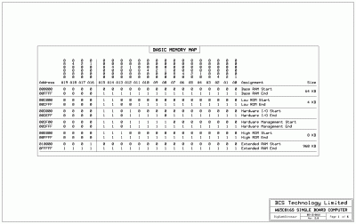
sbc_p1.gif [ 120.09 KiB | Viewed 804 times ]
Attachment:
File comment: POC V2 Schematic: I/O & HMU Decoding
sbc_p2.gif
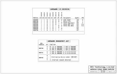
sbc_p2.gif [ 107.8 KiB | Viewed 804 times ]
Attachment:
File comment: POC V2 Schematic: MPU Interface
sbc_p3.gif
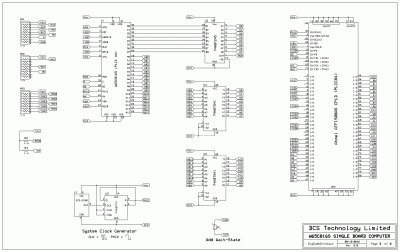
sbc_p3.gif [ 171.26 KiB | Viewed 804 times ]
Attachment:
File comment: POC V2 Schematic: RAM, ROM & I/O
sbc_p4.gif
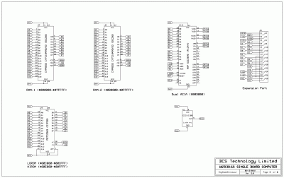
sbc_p4.gif [ 144.2 KiB | Viewed 804 times ]
Attachment:
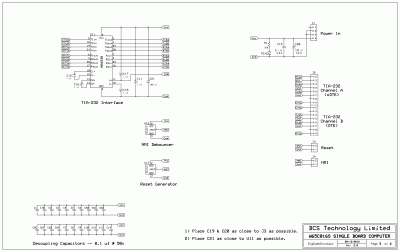
File comment: POC V2 Schematic: External Interface
sbc_p5.gif
sbc_p5.gif [ 107.04 KiB | Viewed 804 times ]

Due to the forum software's five attachment limit per post, the preliminary printed circuit board layout is in the next post.

Salient features of this design are:

  • 1024 KB of RAM, implemented with two 512 KB SRAMs in a flat memory model. Addressing ranges from $000000 to $0FFFFF. Pages 1 and 2 of the schematic give the details. The first 64 KB of RAM is "base RAM" and everything above is "extended RAM." I used those terms so I could easily refer to these ranges in the CPLD code. Functionally speaking, this design could work with just base RAM, but would then effectively be nothing more than POC V1 with faster logic.

  • Glue logic in an Atmel 1508AS CPLD. The 1508AS is a fairly mature product that can support 3.3 or 5 volt I/O operation. The core itself runs at 5 volts. Currently it appears the 1508AS may be a bit of overkill, but that's better than not having sufficient resources. Incidentally, Atmel makes a test rig for this device (and many of their other 1500 series CPLDs) that doubles as a programmer. I decided to invest in one rather than scratch-design and build a JTAG device.

  • Segmented ROM. The $00E000-$00FFFF ROM range will contain reset code, the BIOS and a basic interrupt handler. The $00C000-$00CFFF range will be the new home of the machine language monitor. Either or both ROM segments can be mapped out to expose the RAM below. A write to any ROM address will automatically bleed through to RAM, so the BIOS segment could copy itself to RAM and then map itself out and continue running from RAM. This would be effectively like "BIOS shadowing" in the PC architecture, with a corresponding performance improvement.

  • I/O at $00D000, with eight device selects available. There will also be RAM under the I/O block that can be exposed if for some as-yet-unknown reason I decide that 4 KB chunk of RAM is good for something. Incidentally, the $00C000 and $00E000 RAM blocks can be write-protected in this scheme. Write-protecting the $00E000 block will be important, as the kernel's interrupt handlers and the MPU vectors will be in this range.

  • Hardware memory protection. Once this hardware is working, I may try to see about policing attempts to execute potentially destructive instructions (e.g., stack pointer changes), assuming there are enough P-terms left in the CPLD when everything else has been handled. If I can do that I may be able to solve the bank $00 dilemma.

  • ROM and I/O wait-stating. At any speed above 12.5 MHz wait-stating will be necessary. As the access times of the ROM and I/O devices are about the same, a one-size-fits-all wait-state period should be okay for initial testing. I did wire an external jumper (EWS) into the circuit which, if shorted, will add an extra wait-state without having to reprogram the CPLD.

  • Priority interrupt controller (PIC), with eight IRQs available. I don't actually need that many, but it's a good programming exercise figuring out how to make it work. The interrupt controller will eliminate the need for polling each device to see if it's interrupting, which will certainly help performance. As with the HMU, the interrupt controller is a virtual device within the CPLD. The controller will present an IRQ number ($00-$07) on the data bus when interrogated. The PIC will ultimately yank on the MPU's IRQB input to produce the interrupt. That CPLD output will be actively driven in both directions so slew time in the IRQ circuit doesn't get in the way of high speed interrupt processing (e.g., when an octart has all eight channels going full blast).

  • Active bus drivers. Although these were not present in POC V1, testing has revealed that they will be required in V2. More on this below.

  • Backward compatibility to POC V1—sort of. The physical layout of POC V2's printed circuit board will allow me to plug in my existing SCSI host adapter (HBA). A small patch will have to be made to the HBA to account for the use of separate IRQs for the SCSI controller and the watchdog timer. Otherwise, it'll work like it does in POC V1.

When I had built the first SCSI HBA I quickly found that I had to slow down the Ø2 clock in order for the unit to work. During 'scope observations of POC V1's buses with the SCSI HBA installed, it was soon clear that the MPU was having some trouble driving the buses hard enough to maintain acceptable slew rates. The problem is that the HBA effectively takes the entire data bus and part of the address bus off the mainboard, which unavoidably adds unwanted reactance to the circuit, mostly a lot of stray capacitance. With that capacitive loading in place, the MPU couldn't generate enough drive to slew the data bus at an acceptable rate once Ø2 got over 10 MHz. If the HBA were removed then error-free operation was possible at 15 MHz, although there were timing violations to the I/O hardware that caused occasional funny behavior with the TIA-232 ports.

After mulling this for a while, and mindful that WDC doesn't actually state in the data sheet what the '816's fanout capability is, I concluded that I needed to do something about bus drive. Otherwise, it was a sure bet that the extra loading of the CPLD and two pieces of SRAM would sabotage any attempt to achieve high speed operation. Although it is generally known that the '816's drive strength is better than might be expected, it wouldn't be safe to design around an assumption. So this new design includes 74ABT541 bus drivers for A0-A15 and a 74ABT245 transceiver for D0-D7. ABT logic is exceptionally fast (3-4 ns prop time) and produces high output drive. The only real negative is that there are a few more parts for which to find space on the PCB. I resolved that issue by using SOIC (50 mil) packages.

Naturally, this design will receive more scrutiny before anything gets produced, as it's likely some little oversight is waiting to get me. :lol:

_________________
x86?  We ain't got no x86.  We don't NEED no stinking x86!


Last edited by BigDumbDinosaur on Wed Jun 27, 2012 6:21 am, edited 6 times in total.

Top
 Profile  
Reply with quote  
 Post subject: Re: POC Version 2
PostPosted: Sun Jun 24, 2012 10:34 pm 
Offline
User avatar

Joined: Thu May 28, 2009 9:46 pm
Posts: 8177
Location: Midwestern USA
Here is the printed circuit board layout for POC V2.

Attachment:
File comment: POC V2 PCB Layout
sbc_pcb.png
sbc_pcb.png [ 219.45 KiB | Viewed 805 times ]


Like POC V1, this will be made with EPCB's ProtoPro service. I slightly enlarged the board to make room for extra hardware and to facilitate trace routing. I had to play around with the layout for a while because it kept exceeding the 650 hole limit of the ProtoPro service. Shifting things around allowed me to eliminate unnecessary via. The board is exactly 21 square inches, which is the limit for the ProtoPro service. I will probably play with this some more, since it's likely there's an error somewhere that will need correcting.

_________________
x86?  We ain't got no x86.  We don't NEED no stinking x86!


Last edited by BigDumbDinosaur on Mon Jun 25, 2012 7:34 am, edited 1 time in total.

Top
 Profile  
Reply with quote  
 Post subject: Re: POC Version 2
PostPosted: Mon Jun 25, 2012 3:39 am 
Offline

Joined: Sat Dec 13, 2003 3:37 pm
Posts: 1004
I have no idea what I'm talking about, and am making this up out of whole cloth.

But is there any way for the MMU logic to "know" what the most recent PC was, and to "know" if the most recent PC was located in bank $00, and that if it was then it can open the address bus to the full 24 bits (so the kernel can see everything), vs one of the banks that can only see it's local bank? I don't know if there's a control pin that tells you its fetching an instruction vs a piece of data.


Top
 Profile  
Reply with quote  
 Post subject: Re: POC Version 2
PostPosted: Mon Jun 25, 2012 6:03 am 
Offline

Joined: Sun Nov 08, 2009 1:56 am
Posts: 387
Location: Minnesota
Quote:
Segmentation is not without its drawbacks. Since any process is not allowed to access another process's segment, the time-honored method of accessing a kernel API as a subroutine is out—the JSR would cause a hardware exception by virtue of accessing "privileged" RAM (the kernel's space, in this case). Allowing such access would mean a special case condition would have to exist in the glue logic to allow a JSR to a kernel API address, but nowhere else outside of user process space. A lot of CPLD capability could be eaten up trying to enforce this very narrow access rule, as the data bus would have to be monitored for one unique instruction.


What if the hardware "mirrored" a bit of the kernel in every 64K block? 1K or 512 bytes or something like that at the top of every 64K block? Perhaps just enough code space to save enough context to "know" which process is calling and then switch to the "real" kernel?

I'm reminded of the C128's memory management registers, which appeared as I/O at $FF00+ in all 256 possible configurations, even ones which in theory had no I/O registers at all (thus avoiding the problem of getting "stuck" in a configuration with no way out because of being unable to write to the memory management registers).


Top
 Profile  
Reply with quote  
 Post subject: Re: POC Version 2
PostPosted: Mon Jun 25, 2012 7:38 am 
Offline
User avatar

Joined: Thu May 28, 2009 9:46 pm
Posts: 8177
Location: Midwestern USA
teamtempest wrote:
Quote:
Segmentation is not without its drawbacks. Since any process is not allowed to access another process's segment, the time-honored method of accessing a kernel API as a subroutine is out—the JSR would cause a hardware exception by virtue of accessing "privileged" RAM (the kernel's space, in this case). Allowing such access would mean a special case condition would have to exist in the glue logic to allow a JSR to a kernel API address, but nowhere else outside of user process space. A lot of CPLD capability could be eaten up trying to enforce this very narrow access rule, as the data bus would have to be monitored for one unique instruction.


What if the hardware "mirrored" a bit of the kernel in every 64K block? 1K or 512 bytes or something like that at the top of every 64K block? Perhaps just enough code space to save enough context to "know" which process is calling and then switch to the "real" kernel?

I'm reminded of the C128's memory management registers, which appeared as I/O at $FF00+ in all 256 possible configurations, even ones which in theory had no I/O registers at all (thus avoiding the problem of getting "stuck" in a configuration with no way out because of being unable to write to the memory management registers).

That could be done but it would then be necessary to somehow write-protect the mirrored area, since it would appear to be in part of the user process' space. If kernel APIs are called via software interrupts then mirroring isn't necessary, but then the problem of the kernel accessing the caller's stack gets involved. It's messy, either way.

_________________
x86?  We ain't got no x86.  We don't NEED no stinking x86!


Last edited by BigDumbDinosaur on Mon Jun 25, 2012 7:51 am, edited 1 time in total.

Top
 Profile  
Reply with quote  
 Post subject: Re: POC Version 2
PostPosted: Mon Jun 25, 2012 7:48 am 
Offline
User avatar

Joined: Thu May 28, 2009 9:46 pm
Posts: 8177
Location: Midwestern USA
whartung wrote:
I have no idea what I'm talking about, and am making this up out of whole cloth.

But is there any way for the MMU logic to "know" what the most recent PC was, and to "know" if the most recent PC was located in bank $00, and that if it was then it can open the address bus to the full 24 bits (so the kernel can see everything), vs one of the banks that can only see it's local bank? I don't know if there's a control pin that tells you its fetching an instruction vs a piece of data.

The '816 has outputs(VDA and VPA) that can tell other hardware if the current bus cycle is an opcode fetch, an operand fetch or an invalid bus condition, so that's already available. Having the HMU know what the last PC was would require that it maintain state, which is theoretically possible. However, the PC doesn't actually reflect which bank was accessed. That information is presented on D0-D7 when Ø2 is low and VDA and/or VPA are asserted. If, for example, a program pushes the accumulator, the MPU will generate a bank $00 address in the last cycle of the instruction. Whatever happened before that is not known. If the same program had previously pointed the stack at the I/O block (which would surely cause a crash) there would be no evidence that such a thing was done until an actual stack access occurred. By then, it would be too late to abort the instruction and take control away from the errant process.

It appears that somehow programs (other than the kernel) have to be prevented from changing the stack pointer, direct page (zero page) register and the data bank register. Otherwise, it's open season on any process that happens to get in the way.

_________________
x86?  We ain't got no x86.  We don't NEED no stinking x86!


Last edited by BigDumbDinosaur on Mon Jun 25, 2012 5:52 pm, edited 1 time in total.

Top
 Profile  
Reply with quote  
 Post subject: Re: POC Version 2
PostPosted: Mon Jun 25, 2012 5:51 pm 
Offline
User avatar

Joined: Thu May 28, 2009 9:46 pm
Posts: 8177
Location: Midwestern USA
BigDumbDinosaur wrote:
Naturally, this design will receive more scrutiny before anything gets produced, as it's likely some little oversight is waiting to get me. :lol:

It didn't take long for me to find one of those oversights. Somehow when I was working out the circuitry for the data bus transceiver I neglected to account for one of the three possible data bus conditions. :oops: Guess I shouldn't be working on this stuff so late in the evening.

_________________
x86?  We ain't got no x86.  We don't NEED no stinking x86!


Top
 Profile  
Reply with quote  
 Post subject: Re: POC Version 2
PostPosted: Mon Jun 25, 2012 6:26 pm 
Offline

Joined: Sat Dec 13, 2003 3:37 pm
Posts: 1004
BigDumbDinosaur wrote:
However, the PC doesn't actually reflect which bank was accessed. That information is presented on D0-D7 when Ø2 is low and VDA and/or VPA are asserted. If, for example, a program pushes the accumulator, the MPU will generate a bank $00 address in the last cycle of the instruction. Whatever happened before that is not known. If the same program had previously pointed the stack at the I/O block (which would surely cause a crash) there would be no evidence that such a thing was done until an actual stack access occurred. By then, it would be too late to abort the instruction and take control away from the errant process.

I guess all I was thinking is that Bank $00 can be considered the privileged bank, and each time an opcode is fetched you capture the current bank address for that opcode. When that value is $00, you can set a latch or something.

In the decode logic, when it detects a DATA access is taking place, if the latch is set, then the bank address for the data access can just go through from the DB/BA0-7 pins. If the latch is NOT set, then the data bank address is hidden, and the one that was captured during the opcode fetch is used instead (thus limiting non-privileged banks to their own 64K block).

The security about the DBR is simply that it's effectively ignored and matches the PBR all the time, as enforced by the hardware, save for when running in the kernel space.


Top
 Profile  
Reply with quote  
Display posts from previous:  Sort by  
Post new topic Reply to topic  [ 544 posts ]  Go to page Previous  1 ... 3, 4, 5, 6, 7, 8, 9 ... 37  Next

All times are UTC


Who is online

Users browsing this forum: jds and 5 guests


You cannot post new topics in this forum
You cannot reply to topics in this forum
You cannot edit your posts in this forum
You cannot delete your posts in this forum
You cannot post attachments in this forum

Search for:
Jump to: