6502.org Forum  Projects  Code  Documents  Tools  Forum
It is currently Sat May 04, 2024 3:04 am

All times are UTC


Post new topic Reply to topic  [ 544 posts ]  Go to page Previous  1 ... 13, 14, 15, 16, 17, 18, 19 ... 37  Next
Author Message
 Post subject: Re: POC Version 2
PostPosted: Tue Dec 02, 2014 1:09 am 
Offline

Joined: Mon Mar 02, 2009 7:27 pm
Posts: 3258
Location: NC, USA
BitWise wrote:
Sounds like its time to move to a more open design tool and send the plot files to China.

I don't mean to hi-jack BDDs thread but what design tool are you guys referring to?

_________________
65Org16:https://github.com/ElEctric-EyE/verilog-6502


Top
 Profile  
Reply with quote  
 Post subject: Re: POC Version 2
PostPosted: Tue Dec 02, 2014 5:50 am 
Offline
User avatar

Joined: Thu May 28, 2009 9:46 pm
Posts: 8172
Location: Midwestern USA
ElEctric_EyE wrote:
BitWise wrote:
Sounds like its time to move to a more open design tool and send the plot files to China.

I don't mean to hi-jack BDDs thread but what design tool are you guys referring to?

I'm not sure. If it's Eagle they're referring to that's a lot of money that I don't feel like spending. The EPCB stuff is fine for my needs.

_________________
x86?  We ain't got no x86.  We don't NEED no stinking x86!


Top
 Profile  
Reply with quote  
 Post subject: Re: POC Version 2
PostPosted: Tue Dec 02, 2014 6:41 am 
Offline
User avatar

Joined: Fri Aug 30, 2002 1:09 am
Posts: 8430
Location: Southern California
A few topics on PCB CAD we've had in the past are:
Circuit Design Software Question
PCB programs for Linux
Schematic and PCB software
There's a lot of free CAD software compared at http://en.wikipedia.org/wiki/Comparison_of_EDA_software .

Any standard PCB CAD will produce industry-standard gerber files which you can email to all board manufacturers except the few that want to lock you into their proprietary CAD so you won't go elsewhere. There are countless board houses I could send my past board designs to, many of which may not have even existed yet when I laid out any particular board.

_________________
http://WilsonMinesCo.com/ lots of 6502 resources
The "second front page" is http://wilsonminesco.com/links.html .
What's an additional VIA among friends, anyhow?


Top
 Profile  
Reply with quote  
 Post subject: Re: POC Version 2
PostPosted: Mon Dec 22, 2014 4:36 am 
Offline
User avatar

Joined: Thu May 28, 2009 9:46 pm
Posts: 8172
Location: Midwestern USA
BigDumbDinosaur wrote:
...The caveat about the JTAG pins being used as I/O is that in-circuit programming can't be done. Ironically, with the 1508AS I could have a JTAG port on the board, since I don't need to commit those pins to I/O.

I suppose that the JTAG pins could be used for that purpose as well as I/O pins with the use of some jumper blocks. Of course, jumper blocks add in-circuit capacitance that I'd just as soon avoid.

_________________
x86?  We ain't got no x86.  We don't NEED no stinking x86!


Top
 Profile  
Reply with quote  
 Post subject: Re: POC Version 2
PostPosted: Tue Dec 23, 2014 4:17 am 
Offline
User avatar

Joined: Fri Dec 11, 2009 3:50 pm
Posts: 3350
Location: Ontario, Canada
Since the jumpers would simply act as a double-throw switch, an alternative is to use a 4PDT FET mux. These are available in the familiar 74_257 pinout, but shrunken to SOIC (and smaller). The capability exceeds that of ordinary '257s because FET switches are bidirectional, meaning that any or all of the sections can be used as a demux rather than a mux. This suits the JTAG problem, where a mixture of inputs & outputs must be switched.

Of course you'll need something to drive the device's Select input so it'll know which way to switch. A single jumper + a pullup could accomplish that, or -- better yet -- you might contrive a means by which the switchover happens automatically when the programming cable is attached.

Just throwin' the idea out there... Others may use it even if you don't. :)

-- Jeff

5 volt device: 74CBT3257
3 volt device: 74CBTLV3257

_________________
In 1988 my 65C02 got six new registers and 44 new full-speed instructions!
https://laughtonelectronics.com/Arcana/ ... mmary.html


Top
 Profile  
Reply with quote  
PostPosted: Fri Jun 05, 2015 5:17 am 
Offline
User avatar

Joined: Thu May 28, 2009 9:46 pm
Posts: 8172
Location: Midwestern USA
BigDumbDinosaur wrote:
Okay, I've run into a problem. I have here the Atmel programming/test rig for their CPLDs...POC V2 is going to use the smaller 1504AS, which is in a PLCC-44 package. So a while back, I ordered the PLCC-44 adapter and waited for it to ship. And waited and waited and waited and...

Anyhow there's a snag at Atmel and it doesn't look like I'm going to get this adapter anytime soon.

I received an update from Mouser that my order for this adapter will be fulfilled the middle of next month. Evidently Atmel is producing them again. So...it appears I will be able to build POC V2 as originally designed with the ATF1504AS CPLD, which is a much better fit on the EPCB Proto-Pro board layout than the 1508AS's PLCC-84 package. Ergo I'll sit on this a little longer and see if the programming adapter arrives as promised. At least I have a ship date, which I didn't have before.

BTW, I placed the order for this adapter in January 2014. :?

_________________
x86?  We ain't got no x86.  We don't NEED no stinking x86!


Top
 Profile  
Reply with quote  
PostPosted: Sat Aug 15, 2015 3:46 am 
Offline
User avatar

Joined: Thu May 28, 2009 9:46 pm
Posts: 8172
Location: Midwestern USA
BigDumbDinosaur wrote:
Okay, I've run into a problem. I have here the Atmel programming/test rig for their CPLDs...POC V2 is going to use the smaller 1504AS, which is in a PLCC-44 package. So a while back, I ordered the PLCC-44 adapter and waited for it to ship. And waited and waited and waited and...

Anyhow there's a snag at Atmel and it doesn't look like I'm going to get this adapter anytime soon.

I received an update from Mouser that my order for this adapter will be fulfilled the middle of next month. Evidently Atmel is producing them again. So...it appears I will be able to build POC V2 as originally designed with the ATF1504AS CPLD, which is a much better fit on the EPCB Proto-Pro board layout than the 1508AS's PLCC-84 package. Ergo I'll sit on this a little longer and see if the programming adapter arrives as promised. At least I have a ship date, which I didn't have before.

BTW, I placed the order for this adapter in January 2014. :?

Well, guess what? I received yet another update from Mouser and now the expected ship date has been changed to October. Geesh! :evil: At the rate this is going, my grandchildren will be retired before the adapter arrives.

_________________
x86?  We ain't got no x86.  We don't NEED no stinking x86!


Top
 Profile  
Reply with quote  
 Post subject: Re: POC Version 2
PostPosted: Sat Aug 15, 2015 9:05 am 
Offline
User avatar

Joined: Sun Oct 13, 2013 2:58 pm
Posts: 485
Location: Switzerland
Hi BDD,

why do you wait for the adapter? Build your own JTAG to PLCC-44 Adapter. You don't need the test board, you only need the download cable. The download cable that comes with the test-rig provides a standard JTAG port. You only need to connect the supply pins (GND VCC) of the ATF1504AS and connect it to 5V and then connect the GND and VCC with the 4 JTAG signals TMS, TMO, TMI, TCK to the JTAG port. This even works when you just use some Dupont wires. I did the same for the first tests of my USB download cable. You could even build a small strip-board with a 10-pin header and a PLCC-44 adapter and a 5V Power Connection and that's all you need with your download cable to program the ATF1504AS, and when you put a PLCC-84 Adapter on the same strip-board and make the correct connections then you can program both, as an ultimate solution you could even cascade the adapters and provide jumpers to short cut the adapter without a CPLD (just connect TMI to TMO of the empty adapter). You should also consider a JTAG pin-header on your POC, so you can even program the ATF when it is inserted in the board. Just connect the down-load cable with a 10-pin ribbon cable and that's it.

Cheers

Peter


Top
 Profile  
Reply with quote  
 Post subject: Re: POC Version 2
PostPosted: Mon Aug 31, 2015 8:43 pm 
Offline
User avatar

Joined: Thu May 28, 2009 9:46 pm
Posts: 8172
Location: Midwestern USA
cbscpe wrote:
You should also consider a JTAG pin-header on your POC, so you can even program the ATF when it is inserted in the board.

Your suggestion was my command. :lol:

I went over the whole of POC V2's design and reverted it to the Atmel ATF1504AS CPLD, which is in a PLCC44 package. A JTAG port has been added and new logic written. Unless a mistake in design or PCB layout is found in the next few days, this will be the "production" design, and PCBs and parts will be ordered.

Illustrations follow in this post and the next one. Some additional commentary will follow the last illustration.

Attachment:
File comment: POC V2 Schematic, Page 1: Architecture
sbc_1504asP1.gif
sbc_1504asP1.gif [ 68.32 KiB | Viewed 809 times ]
Attachment:
File comment: POC V2 Schematic, Page 2: Memory Map
sbc_1504asP2.gif
sbc_1504asP2.gif [ 129.37 KiB | Viewed 809 times ]
Attachment:
File comment: POC V2 Schematic, Page 3: I/O Map
sbc_1504asP3.gif
sbc_1504asP3.gif [ 72.99 KiB | Viewed 809 times ]
Attachment:
File comment: POC V2 Schematic, Page 4:, MPU Interface
sbc_1504asP4.gif
sbc_1504asP4.gif [ 130.62 KiB | Viewed 809 times ]
Attachment:
File comment: POC V2 Schematic, Page 5: RAM, ROM & I/O
sbc_1504asP5.gif
sbc_1504asP5.gif [ 139.71 KiB | Viewed 809 times ]

_________________
x86?  We ain't got no x86.  We don't NEED no stinking x86!


Last edited by BigDumbDinosaur on Mon Aug 31, 2015 10:13 pm, edited 1 time in total.

Top
 Profile  
Reply with quote  
 Post subject: Re: POC Version 2
PostPosted: Mon Aug 31, 2015 10:13 pm 
Offline
User avatar

Joined: Thu May 28, 2009 9:46 pm
Posts: 8172
Location: Midwestern USA
Continuing with illustrations...

Attachment:
File comment: POC V2 Schematic, Page 6: External Interface
sbc_1504asP6.gif
sbc_1504asP6.gif [ 166.93 KiB | Viewed 803 times ]
Attachment:
File comment: POC V2 Printed Circuit Board: Composite View
sbc_1504asPCB.gif
sbc_1504asPCB.gif [ 111.23 KiB | Viewed 803 times ]
Attachment:
File comment: POC V2 Printed Circuit Board: Silkscreen View
sbc_1504asPCBss.gif
sbc_1504asPCBss.gif [ 42.61 KiB | Viewed 803 times ]
Attachment:
File comment: POC V2 Printed Circuit Board: Top Copper View
sbc_1504asPCBtop.gif
sbc_1504asPCBtop.gif [ 58.35 KiB | Viewed 803 times ]
Attachment:
File comment: POC V2 Printed Circuit Board: Bottom Copper View
sbc_1504asPCBbot.gif
sbc_1504asPCBbot.gif [ 44.09 KiB | Viewed 803 times ]

Comments:

  • I replaced the unit's Molex 5¼ inch floppy drive power receptacle with the smaller Berg style 3½ inch floppy disk receptacle to reduce footprint. I also added a mounting hole in the vicinity of the expansion port socket for improved board rigidity.

  • The SCSI host adapter that is presently attached to POC V1 is 100 percent compatible with this unit.

  • There are four TIA-232 serial communications ports, all of which can be simultaneously operated at speeds up to 230.4 Kbps, with full hardware handshaking. As with POC V1, port A is the console port and port B is for interconnection to my UNIX software development box. Ports C and D are uncommitted at this time.

  • The UART in this unit is NXP's 28C94, which has eight-deep FIFOs on both receive and transmit. The 28C94 is essentially a scaled-up version of the dual-channel 26C92, and can be operated in x86 or Motorola 68K bus mode. Oddly enough, x86 mode is easier to interface to the 65C816, even though the read/write logic is a little more involved. :?

  • The console port can be configured to operate at TIA-232 or TTL levels by moving around some jumpers on the PCB (JP3 and JP4). This arrangement will allow me to either connect a standard dumb terminal via TIA-232, as I am now doing, or attach a MicroVGA serial controller (or similar) to the unit. The circuit is designed so that when the latter configuration is in use the DTR output becomes Vcc for powering external hardware.

  • As with POC V1, Ø2 is generated by running the clock oscillator through a 74ABT74 flop. I used an SOIC package for that device to save space. The 512KB SRAM is in an SOJ package similar to the 128KB SRAM on POC V1, which I can manually solder with little trouble.

  • In reverting back to the ATF1504AS CPLD, I had to come to grips with the relatively small number of uncommitted I/O pins on the device, 32 maximum if JTAG is to be used. The device's 64 macrocells are more than adequate for my logic requirements, but the limited pin count meant I had to choose my connections quite carefully. Also, while it was temping to assign pins on the basis of how easy they were to connect to other parts of the circuit, it wasn't possible to get the logic design to fit the device using that strategy.

    My approach was to write the logic with no pin numbers assigned, except for the reset and Ø2 inputs (which are essentially immutable), and then after successful compilation and simulation of the design, use the pins that were assigned by the fitter software. It meant a fair amount of rerouting on the PCB, but everything that I wanted to connect to the CPLD is connected and should work as intended. I also made extensive use of pin nodes to facilitate buried logic, such as the bank address latches.

  • Going back to the limited number of I/O pins on the CPLD, the maximum amount of RAM that can be addressed is 512KB. This is due to the fact that only data lines D0-D2 are attached to the CPLD. Hence the maximum number of banks that can be decoded and latched is eight, support a maximum address of $07FFFF or 524,287. Also implied, only three bits are possible in the "hardware management unit" (HMU, more on this below), since only three bits of data will be available

  • The CPLD logic includes provisions for an HMU, which will be able to change the memory map in the address range $00C000-$00FFFF. The first logic design will map ROM and I/O in that range and while the HMU will accept bit patterns it will not affect the map. Once I've got a working unit I will complete the HMU logic that will make it possible to map out ROM at $00C000-$00CFFF and/or $00E000-$00FFFF, as well as map out I/O at $00D000-$00DEFF and replace these ranges with RAM. The HMU, which will appear at $00DF00, can never be mapped out. The front ends of the interrupt service routines will have to be careful to map in I/O in case it is mapped out when an IRQ or NMI hits. As the HMU is read/write, the ISR can read the configuration, push it and do an STZ to establish the default map.

  • As only bits 0-2 in the HMU will be connected to the data bus during a read on that register, I added weak pull-down resistors (RN2 on page four of the schematic) to the data bus to sink D3-D7. Otherwise, those lines will float and likely retain their previous content during the brief period when the read operation is in progress. Assuming I'm right on this, a read of the HMU should find bits 3-7 cleared, eliminating the need to mask them to get the true HMU content.

  • Lastly, I think my physical layout is tight enough to support 20 MHz operation. Excepting the I/O hardware, everything operates down near 10 nanoseconds, and the CPLD has the logic required to generate wait-states on the I/O block. So I'm hopeful once I've got this contraption running to be able to plug in a 40 MHz clock oscillator and see full speed ahead.

_________________
x86?  We ain't got no x86.  We don't NEED no stinking x86!


Top
 Profile  
Reply with quote  
 Post subject: POC Version 2
PostPosted: Thu Sep 03, 2015 6:42 am 
Offline
User avatar

Joined: Thu May 28, 2009 9:46 pm
Posts: 8172
Location: Midwestern USA
Concurrently with the redesign of POC V2's PCB, I've been working on the CPLD code needed to make it work. My goals aren't too lofty, mostly just latching of the bank address, generation of appropriate chip selects, generating wait-states on ROM and I/O hardware accesses, etc. I originally was going to make it very simple but after compiling the code and simulating it, decided to get a little more advanced.

The address ranges $00C000-$00CFFF and $00E000-$00FFFF can be made to have either RAM or ROM. Also, the range $00D000-$00DEFF can be made to have I/O or RAM. The "hardware management unit" (HMU) in the CPLD, which is always present at $00DF00, accepts a bit pattern that sets the memory mapping rules. The architecture is as follows:

Code:
           +--------------------------+ $07FFFF
           |                          |
           |       RAM (448 KB)       |
           |                          |
   +-------+--------------------------+ $010000
   |       |                          |
   | E-RAM |       E-ROM (8 KB)       |
   |       |                          |
   +-------+--------------------------+ $00E000
           | Hardware Management Unit |
   +-------+--------------------------+ $00DF00
   |       |                          |
   | D-RAM |       I/O (3.75 KB)      |
   |       |                          |
   +-------+--------------------------+ $00D000
   |       |                          |
   | C-ROM |       C-RAM (4 KB)       |
   |       |                          |
   +-------+--------------------------+ $00C000
           |                          |
           |       RAM (48 KB)        |
           |                          |
           +--------------------------+ $000000

In order to control all this, the HMU is programmed as follows:

Code:
  HMU               
Register   Address   Register Description    Bit  Function
----------------------------------------------------------
hmumcfg    $00DF00   System configuration:    0   0: I/O
                                                  1: D-RAM
                                              1   0: C-RAM
                                                  1: C-ROM
                                              2   0: E-ROM
                                                  1: E-RAM
----------------------------------------------------------

The default memory map following a hard reset is C-RAM, I/O and E-ROM. As the HMU is read/write, instructions such as TRB and TSB may be used to quickly change the map. An STZ instruction on the HMU is all that is required to re-establish the default map.

Logic rules are such that a write to C-ROM or E-ROM will "bleed through" to RAM, making it possible, for example, to copy the E-ROM firmware to RAM with the MVN instruction and then map out E-ROM and continue in RAM. Running the firmware that way will be faster because ROM accesses incur a wait-state. I also wanted to make it possible to write-protect E-RAM, but couldn't fit the design with that feature. Maybe next time... :(

Here are some logic simulation results. Signals that are in yellow are manipulated by the simulator. Red and green signals represent inputs or outputs from devices other than the CPLD.
Attachment:
File comment: E-ROM & E-RAM Accesses
logic_sim_rom_ram_run.gif
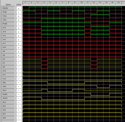
logic_sim_rom_ram_run.gif [ 33.09 KiB | Viewed 764 times ]

In the above, starting at vector 4 and ending at vector 10, a read access of E-ROM is made. Note the generation of a 1 cycle wait-state when ROM is selected. Note that D0-D2 are %000 during Ø2 low at vector 4, as the address from which data is being fetched is $00E000. It can be seen that the simulator has asserted the /RD signal, qualified by Ø2, and that the MPU's RDY input is negated for a full clock cycle, starting at vector 5. This is the wait-state that occurs on all ROM accesses.

At vector 12, a write to the same address occurs. As the logic causes a write on a ROM address to be directed to RAM, RAM is selected and there is no wait-state. Again, D0-D2 are %000 during Ø2 low at vector 12. Also note that the /WD output is asserted, as this is a write operation. As with /RD, /WD is qualified by Ø2.

Attachment:
File comment: Extended RAM Accesses
logic_sim_ext_ram_run.gif
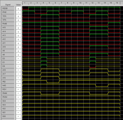
logic_sim_ext_ram_run.gif [ 33.23 KiB | Viewed 764 times ]

In the above and starting at vector 4, data is fetched from "extended" RAM at $07FFFF. Starting at vector 12, data is written to extended RAM at $06E500. Note the conditions of the A16-A18 outputs during the operations.

Attachment:
File comment: I/O Device 'A' Access
logic_sim_IO_run.gif
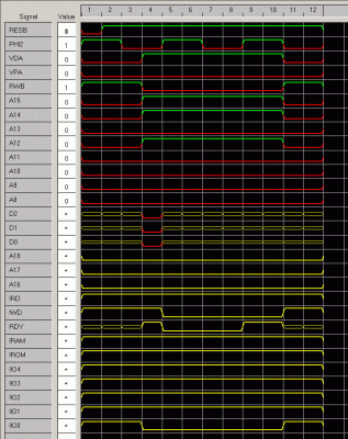
logic_sim_IO_run.gif [ 51.42 KiB | Viewed 764 times ]

In the above, a write access to I/O device 'A' (the real-time clock) is being made. Note that I/O also incurs a wait-state, again lasting a clock cycle. As I have successfully run POC V1.1 at 12.5 MHz, it follows that a single-cycle wait-state should be sufficient for all I/O devices, even at 20 MHz.

Attachment:
File comment: I/O Device 'C' Access
logic_sim_IO_C_run.gif
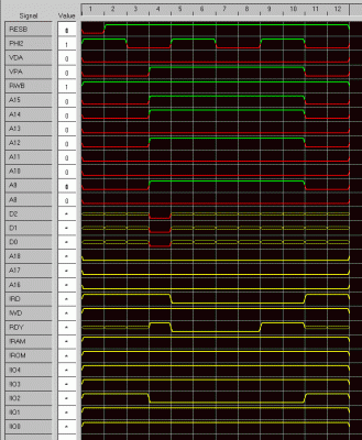
logic_sim_IO_C_run.gif [ 27.74 KiB | Viewed 764 times ]

In the above, a read access on I/O device 'C' is performed. Behavior is like that of the previous simulation run, except a different chip select output is asserted and, of course, /RD is asserted instead of /WD.

Here is the CUPL code that makes all this work:

Code:
/*
* * * * * * * * * * * * * * * * * * * * * * * * * * * * * * * * * * * * * * * * * *
*                                                                                 *
*                 W65C816S PROOF OF CONCEPT SINGLE-BOARD COMPUTER                 *
*                                                                                 *
* =============================================================================== *
*                                                                                 *
*        Copyright (c)2015 by BCS Technology Limited.  All rights reserved.       *
*                                                                                 *
* Permission is hereby granted to use, copy, modify and distribute this software, *
* provided this copyright notice remains unaltered in the source code and  proper *
* attribution is given.  Redistribution, in any form, must be at no charge to the *
* end user.  This code or any part  thereof, including any derivation, MAY NOT be *
* incorporated into any package intended for sale unless written permission to do *
* so has been granted by the copyright holder.                                    *
* ------------------------------------------------------------------------------- *
* THERE IS NO WARRANTY OF ANY KIND WITH THIS SOFTWARE.                            *
*                                                                                 *
* While it is believed that all code will perform as intended,  the user  assumes *
* all risk in connection with the incorporation of this software into any system. *
*                                                                                 *
* * * * * * * * * * * * * * * * * * * * * * * * * * * * * * * * * * * * * * * * * *

* * * * * * * * * *
* VERSION HISTORY *
* * * * * * * * * *

Ver    Rev Date    Revision
--------------------------------------------------------------------------------
0.1.0  2015/08/21  Original version.
--------------------------------------------------------------------------------
*/

Name        glue;
PartNo      B402170001;
Date        2015/08/21;
Revision    0.1.0;
Designer    BDD;
Company     BCS Technology Limited;
Assembly    POC V2;
Location    U2;
Device      f1504ispplcc44;                       /* ATF1504AS (PLCC44):

                                 R     P
                        R  V  A  E  V  H  G  A  A
                  W  R  O  C  1  S  P  I  N  1  1
                  D  D  M  C  2  B  B  2  D  1  0
               ____________________________________
              /   6  5  4  3  2  1 44 43 42 41 40  \
  (JTAG) TDI |  7                                39 | A9
          D2 |  8                                38 | TDO (JTAG)
          D1 |  9                                37 | A8
         GND | 10                                36 | N/C
          D0 | 11                                35 | VCC
         IO0 | 12                                34 | VDA
  (JTAG) TMS | 13                                33 | VPA
         RAM | 14                                32 | TCK (JTAG)
         VCC | 15                                31 | A18
         RDY | 16                                30 | GND
         IO1 | 17                                29 | A16
             |   18 19 20 21 22 23 24 25 26 27 28   |
              \____________________________________/
                  I  A  I  I  G  V  A  A  A  R  R
                  O  1  O  O  N  C  1  1  1  W  S
                  3  7  2  4  D  C  3  4  5  B  T

*/

property   atmel {cascade_logic=on};
property   atmel {logic_doubling=on};
property   atmel {output_fast=on};
property   atmel {pin_keep=off};
property   atmel {preassign=keep};
property   atmel {security=off};
property   atmel {xor_synthesis=on};

/*
=====================
INPUT PIN ASSIGNMENTS
=====================
*/
pin  1    = RESB;                                 /* system reset              */
pin  2    = A12;                                  /* address line              */
pin 24    = A13;                                  /* address line              */
pin 25    = A14;                                  /* address line              */
pin 26    = A15;                                  /* address line              */
pin 27    = RWB;                                  /* read/write                */
pin 33    = VPA;                                  /* valid instruction address */
pin 34    = VDA;                                  /* valid data address        */
pin 37    = A8;                                   /* address line              */
pin 39    = A9;                                   /* address line              */
pin 40    = A10;                                  /* address line              */
pin 41    = A11;                                  /* address line              */
pin 43    = PHI2;                                 /* system clock              */
pin 44    = VPB;                                  /* interrupt vector pull     */

/*
======================
OUTPUT PIN ASSIGNMENTS
======================
*/
pin  4    = !ROM;                                 /* ROM chip select       */
pin  5    = !RD;                                  /* read data             */
pin  6    = !WD;                                  /* write data            */
pin 12    = !IO0;                                 /* I/O device 'A' select */
pin 14    = !RAM;                                 /* RAM chip select       */
pin 17    = !IO1;                                 /* I/O device 'B' select */
pin 18    = !IO3;                                 /* I/O device 'D' select */
pin 19    = A17;                                  /* address line          */
pin 20    = !IO2;                                 /* I/O device 'C' select */
pin 21    = !IO4;                                 /* I/O device 'E' select */
pin 28    = !RST;                                 /* inverted reset        */
pin 29    = A16;                                  /* address line          */
pin 31    = A18;                                  /* address line          */

/*
=============================
BIDIRECTIONAL PIN ASSIGNMENTS
=============================
*/
pin  8    = D2;                                   /* data line */
pin  9    = D1;                                   /* data line */
pin 11    = D0;                                   /* data line */
pin 16    = RDY;                                  /* MPU wait  */

/*
==========================================================
MACHINE ARCHITECTURE & HARDWARE MANAGEMENT UNIT DEFINTIONS
==========================================================

           +--------------------------+ $07FFFF
           |                          |
           |       RAM (448 KB)       |
           |                          |
   +-------+--------------------------+ $010000
   |       |                          |
   | E-RAM |       E-ROM (8 KB)       |
   |       |                          |
   +-------+--------------------------+ $00E000
           | Hardware Management Unit |
   +-------+--------------------------+ $00DF00
   |       |                          |
   | D-RAM |       I/O (3.75 KB)      |
   |       |                          |
   +-------+--------------------------+ $00D000
   |       |                          |
   | C-ROM |       C-RAM (4 KB)       |
   |       |                          |
   +-------+--------------------------+ $00C000
           |                          |
           |       RAM (48 KB)        |
           |                          |
           +--------------------------+ $000000

                1 KB = 1024 bytes


  HMU               
Register   Address   Register Description    Bit  Function
----------------------------------------------------------
hmumcfg    $00DF00   System configuration:    0   0: I/O
                                                  1: D-RAM
                                              1   0: C-RAM
                                                  1: C-ROM
                                              2   0: E-ROM
                                                  1: E-RAM
----------------------------------------------------------
Notes:  1) The default map following hard reset is C-RAM, I/O & E-ROM.
        2) An STZ instruction on hmumcfg sets the default map.
        3) Writing to C-ROM or E-ROM touches RAM at same address.
        4) The HMU is read/write & always present.

*/

$DEFINE   dblkmap   hmumcfg0                      /* $00D0xx-$00DExx */
$DEFINE   cblkmap   hmumcfg1                      /* $00C0xx-$00CFxx */
$DEFINE   eblkmap   hmumcfg2                      /* $00E0xx-$00FFxx */

/*
=========================
BURIED LOGIC DECLARATIONS
=========================
*/
pinnode   = bank0;                                /* 1 = address is $000000-$00FFFF       */
pinnode   = basram;                               /* 1 = address is $000000-$00BFFF       */
pinnode   = cblk;                                 /* 1 = address is $00C000-$00CFFF       */
pinnode   = dblk;                                 /* 1 = address is $00D000-$00DFFF       */
pinnode   = eblk;                                 /* 1 = address is $00E000-$00FFFF       */
pinnode   = extram;                               /* 1 = address is $010000-$07FFFF       */
pinnode   = hmusel;                               /* 1 = HMU being accessed               */
pinnode   = ioblk;                                /* 1 = I/O address space being accessed */
pinnode   = iosel;                                /* 1 = I/O device being accessed        */
pinnode   = mcfgsel;                              /* 1 = HMU configuration being accessed */
pinnode   = ramsel;                               /* 1 = RAM being accessed               */
pinnode   = rdflag;                               /* 1 = data fetch in progress           */
pinnode   = rdyout;                               /* 1 = MPU wait-stated                  */
pinnode   = rhflag;                               /* 1 = data fetch on high clock         */
pinnode   = romsel;                               /* 1 = ROM being accessed               */
pinnode   = vbus;                                 /* 1 = address bus valid                */
pinnode   = vplatch;                              /* 1 = hardware vector being accessed   */
pinnode   = wdflag;                               /* 1 = data store in progress           */
pinnode   = wsflag;                               /* 1 = wait-state in progress           */
pinnode   = wsff;                                 /* wait-state flip-flop                 */
pinnode   = [blatch0..2];                         /* bank address latches                 */
pinnode   = [hmumcfg0..2];                        /* HMU hardware configuration register  */

/*
=========================
REGISTER RESETS & PRESETS
=========================
*/
$REPEAT i = [0..2]
    hmumcfg{i}.AR = !RESB;
/*    hmumcfg{i}.AP = 'b'0; */
$REPEND
vplatch.AR  = !RESB;
wsff.AR     = !RESB;
vplatch.AP  = 'b'0;                         
wsff.AP     = 'b'0;

/*
==========================
INTERMEDIATE CONTROL LOGIC
==========================
*/
phi1       = !PHI2;                               /* inverted system clock       */
vbus       = (VDA #  VPA) & RESB;                 /* true if valid address       */
rdflag     = RWB & vbus;                          /* true if fetch operation     */
rhflag     = rdflag & PHI2;                       /* true if fetch on high clock */
wdflag     = !RWB & vbus;                         /* true if store operation     */

/* vector pull stuff is experimental; it's not actually in use... */

vplatch.LE = !VPB;                                /* open vector pull latch      */
vplatch.L  = VPB;                                 /* indicate vector pull        */

/*
=============================
EXTENDED RAM ADDRESSING LOGIC
=============================

Bits 0-2 of the extended address are captured during a valid bus cycle while
the clock is low.  In the event a wait-state is in progress when the clock
goes low the bank latches will not be disturbed.
*/
[blatch0..2].LE = vbus & phi1 & !rdyout;          /* open latches         */
[blatch0..2].L  = vbus & phi1 & [D0..2];          /* capture bank         */
bank0     = [blatch0..2]:'b'000;                  /* 1 if bank is $00     */
extram    = !bank0;                               /* 1 if bank is $01-$07 */


/*
====================
MEMORY MAPPING LOGIC
====================
*/
basram    = (!A15 # !A14) & bank0;                /* true if $000000-$00BFFF  */
cblk      = A15 & A14 & !(A13 # A12) & bank0;     /* true if $00C000-$00CFFF  */
dblk      = A15 & A14 & !A13 & A12 & bank0;       /* true if $00D000-$00DFFF  */
eblk      = A15 & A14 & A13 & bank0;              /* true if $00E000-$00FFFF  */
ioblk     = dblk & !(A11 & A10 & A9 & A8);        /* true if $00D000-$00DEFF  */

/* RAM selection rules... */

ramsel    = basram #                              /* base RAM, or...        */
            cblk & (!RWB # !cblkmap) #            /* C-RAM if mapped, or... */
            ioblk & dblkmap #                     /* D-RAM if mapped, or... */
            eblk & (!RWB # eblkmap) #             /* E-RAM if mapped, or... */
            extram;                               /* extended RAM           */

/* ROM selection rules... */

romsel    = cblk & RWB & cblkmap #                /* C-ROM if mapped, or... */
            eblk & RWB & !eblkmap;                /* E-ROM if mapped        */

/* I/O devices selection rules... */

iosel     = ioblk & !dblkmap;                     /* $00D0xx-$00DExx if mapped */

/* HMU selection rules... */

hmusel    = dblk & A11 & A10 & A9 & A8;           /* $00DFxx, always present */
mcfgsel   = hmusel;                               /* configuration    */

/*
================
WAIT-STATE LOGIC
================
*/
wsflag    = (iosel # romsel) & vbus;              /* wait-state if I/O or ROM & enabled */
wsff.CK   = PHI2 & wsflag;
wsff.D    = wsff & wsflag;
rdyout    = wsff & wsflag;

/*
=========================
CONTROL OUTPUT STATEMENTS
=========================
*/
[A16..18] = [blatch0..2] & vbus;                  /* A16-A18 address bits       */
IO0       = iosel & !A10 & !A9 & !A8 & vbus;      /* I/O device 'A' select      */
IO1       = iosel & !A10 & !A9 &  A8 & vbus;      /* I/O device 'B' select      */
IO2       = iosel & !A10 &  A9 & !A8 & vbus;      /* I/O device 'C' select      */
IO3       = iosel & !A10 &  A9 &  A8 & vbus;      /* I/O device 'D' select      */
IO4       = iosel &  A10 & !A9 & !A8 & vbus;      /* I/O device 'E' select      */
RAM       = ramsel & vbus;                        /* RAM chip enable            */
RD        = rdflag & (PHI2 # rdyout) & !hmusel;   /* active low read            */
RDY       = !rdyout;                              /* MPU wait-state input       */
RDY.oe    = wsflag;                               /* active if wait-stating     */
ROM       = romsel & vbus;                        /* ROM chip enable            */
RST       = RESB;                                 /* inverted reset             */
WD        = wdflag & (PHI2 # rdyout) & !hmusel;   /* active low write           */

/*
============================
HMU REGISTER READ STATEMENTS
============================
*/
[D0..2].oe = mcfgsel & rhflag;                    /* enable output on D0-D2 */
[D0..2]    = mcfgsel & [hmumcfg0..2] & rhflag;    /* HMU bit pattern on D0-D2 */

/*
=============================
HMU REGISTER WRITE STATEMENTS
=============================
*/
[hmumcfg0..2].LE = mcfgsel & wdflag & PHI2;       /* open HMU latches */
[hmumcfg0..2].L  = mcfgsel & [D0..2] &            /* D0-D2 bit pattern on HMU */
                   wdflag & PHI2;

/* * * * *   E N D   O F   F I L E   * * * * */

The simulator says it will fly. Now I have to build it and hope the simulator is right!

_________________
x86?  We ain't got no x86.  We don't NEED no stinking x86!


Top
 Profile  
Reply with quote  
PostPosted: Tue Oct 13, 2015 7:33 pm 
Offline
User avatar

Joined: Thu May 28, 2009 9:46 pm
Posts: 8172
Location: Midwestern USA
BigDumbDinosaur wrote:
Okay, I've run into a problem. I have here the Atmel programming/test rig for their CPLDs...POC V2 is going to use the smaller 1504AS, which is in a PLCC-44 package. So a while back, I ordered the PLCC-44 adapter and waited for it to ship. And waited and waited and waited and...

Anyhow there's a snag at Atmel and it doesn't look like I'm going to get this adapter anytime soon.

I received an update from Mouser that my order for this adapter will be fulfilled the middle of next month. Evidently Atmel is producing them again. So...it appears I will be able to build POC V2 as originally designed with the ATF1504AS CPLD, which is a much better fit on the EPCB Proto-Pro board layout than the 1508AS's PLCC-84 package. Ergo I'll sit on this a little longer and see if the programming adapter arrives as promised. At least I have a ship date, which I didn't have before.

BTW, I placed the order for this adapter in January 2014. :?

Well, guess what? I received yet another update from Mouser and now the expected ship date has been changed to October. Geesh! :evil: At the rate this is going, my grandchildren will be retired before the adapter arrives.

Oh, the wonders of the Lord! :lol: The Atmel PLCC44 test rig adapter arrived this morning!

Of course, I have already reworked POC V2's design to add a JTAG port so I can program the CPLD in-circuit. However, having the adapter means I can program the CPLD externally, which is good for a first test, as it should eliminate the JRAG interface from the list of things that can malfunction. Once I'm satisfied that my CPLD logic is working I can try out my JTAG port to see if it actually works.

With the acquisition of this new adapter, I now have adapters for PLCC44, TQFP44 and PLCC84 CPLDs.

Attachment:
File comment: Atmel Test Rig PLCC44 Adapter
atmel_adapter_plcc44.gif
atmel_adapter_plcc44.gif [ 1.44 MiB | Viewed 692 times ]
Attachment:
File comment: Atmel Test Rig w/PLCC44 Adapter Installed
test_rig01.gif
test_rig01.gif [ 1.14 MiB | Viewed 692 times ]
Attachment:
File comment: Atmel Test Rig w/PLCC44 Adapter Installed
test_rig02.gif
test_rig02.gif [ 834.8 KiB | Viewed 692 times ]

_________________
x86?  We ain't got no x86.  We don't NEED no stinking x86!


Top
 Profile  
Reply with quote  
 Post subject: Re: POC Version 2
PostPosted: Tue Oct 13, 2015 8:27 pm 
Offline
User avatar

Joined: Thu Dec 11, 2008 1:28 pm
Posts: 10793
Location: England
LEDs, buttons, seven segment displays - you have everything!


Top
 Profile  
Reply with quote  
 Post subject: Re: POC Version 2
PostPosted: Tue Oct 13, 2015 9:42 pm 
Offline
User avatar

Joined: Thu May 28, 2009 9:46 pm
Posts: 8172
Location: Midwestern USA
BigEd wrote:
LEDs, buttons, seven segment displays - you have everything!

I suspect those would be most useful when cobbling up state machines and trying them out. Each device adapter brings out all the signal pins for the relevant package, as well as directing many of them to the main test rig.

_________________
x86?  We ain't got no x86.  We don't NEED no stinking x86!


Top
 Profile  
Reply with quote  
 Post subject: POC Version 2
PostPosted: Tue Oct 20, 2015 12:46 am 
Offline
User avatar

Joined: Thu May 28, 2009 9:46 pm
Posts: 8172
Location: Midwestern USA
POC V2 is getting closer to being built. I've received all parts for it, except PCBs, the latter which will get ordered after I've completed a trial run on reflowing SMT parts, using a left over POC V1.1 board as the victim. I've also used the Atmel test rig adapter to program and verify an ATF1504AS CPLD, and it appears with the testing I did on the test rig that the CPLD is working.

The reflow trial run suffered a setback when the old Proctor-Silex toaster-oven I was intending to use went DOA on me. The main heating element opened up and when I looked into getting a new element, I discovered that the replacement was only slightly cheaper than getting a new toaster-oven. So a new toaster-oven is on the way and the old one is now in someone's scrap pile. :cry:

_________________
x86?  We ain't got no x86.  We don't NEED no stinking x86!


Last edited by BigDumbDinosaur on Tue Oct 20, 2015 4:04 pm, edited 1 time in total.

Top
 Profile  
Reply with quote  
Display posts from previous:  Sort by  
Post new topic Reply to topic  [ 544 posts ]  Go to page Previous  1 ... 13, 14, 15, 16, 17, 18, 19 ... 37  Next

All times are UTC


Who is online

Users browsing this forum: Google [Bot] and 14 guests


You cannot post new topics in this forum
You cannot reply to topics in this forum
You cannot edit your posts in this forum
You cannot delete your posts in this forum
You cannot post attachments in this forum

Search for:
Jump to: