6502.org Forum  Projects  Code  Documents  Tools  Forum
It is currently Sat May 04, 2024 4:35 am

All times are UTC


Post new topic Reply to topic  [ 544 posts ]  Go to page Previous  1 ... 9, 10, 11, 12, 13, 14, 15 ... 37  Next
Author Message
 Post subject: Re: POC Version 2
PostPosted: Sun Nov 18, 2012 7:50 am 
Offline
User avatar

Joined: Thu May 28, 2009 9:46 pm
Posts: 8172
Location: Midwestern USA
enso wrote:
How is Picasso visually?

Please see attached pictures. The first one is a monkey-rig test setup that I used to power the µVGA module to see if it would work. It's hooked up to a 19 inch 4×3 Viewsonic LCD monitor. The second picture is the default splash screen produced by the module if it doesn't receive the AUTOBAUD command within five seconds of being powered on. I think the fonts look fairly similar to what one might see from a PC video card. The last picture is a closeup of the module—as you can see by judging it against the DB-15 monitor connector, it's quite small.

Attachment:
File comment: Picasso µVGA Test Setup
picasso_001.jpg
picasso_001.jpg [ 730.76 KiB | Viewed 1125 times ]

Attachment:
File comment: Splash Screen
picasso_002.jpg
picasso_002.jpg [ 663.73 KiB | Viewed 1125 times ]

Attachment:
File comment: Closeup of µVGA Module
picasso_003.jpg
picasso_003.jpg [ 95.93 KiB | Viewed 1125 times ]

_________________
x86?  We ain't got no x86.  We don't NEED no stinking x86!


Top
 Profile  
Reply with quote  
PostPosted: Tue Apr 30, 2013 5:39 pm 
Offline
User avatar

Joined: Thu May 28, 2009 9:46 pm
Posts: 8172
Location: Midwestern USA
One of the great things about a paper computer is that changing the design involves no solder or wrestling with dinky parts. Of course, a paper computer can't compute, so it's somewhat limited in usefulness.

POC V2 continues to stay in the paper form because the design has been a moving target. Part of the reason for that is the project has already existed for some two years but represents about a month's worth of progress. My goals for this unit aren't as well defined as they were for POC V1, and I continue to tinker with V1 because I have working hardware, which steals time from developing V2. Also, I seem to be having trouble as of late concentrating time on POC stuff in general due to business demands (and health problems), even though I had planned to start winding down business things last year.

Anyhow, I have a little better focus on how POC V2 will be designed and have committed to using programmable logic in the form of an Atmel 1508as CPLD. The 1508as will have a lot to do, so I have to get logic written and simulated before I can proceed with final circuit design and construction. I will also integrate the SECONS µVGA module for console operation, which doesn't actually change the basic design very much (it's a serial I/O device), but does affect the physical PCB layout.

One of the areas that has been in a state of flux is the memory map. My original design was going to use a 512KB SRAM directly attached to the PCB—512K is enough room to support a preemptive kernel, along with disk buffers and other assorted data structures that the kernel would need. Then I figured that if one SRAM was good, two should be better, resulting a 1MB design. However, around that time, Garth released his 4MB DIMM and Daryl subsequently tested it and achieved good results. So I decided to integrate the DIMM into POC V2, resulting in a substantial change to the proposed memory map, which now looks like this:
Attachment:
File comment: POC V2 Memory Map
poc_v2_mem_map.gif
poc_v2_mem_map.gif [ 40.41 KiB | Viewed 1058 times ]
As can be seen in the above, ROM and I/O will be present in the usual places, but can be mapped out to expose RAM at the same addresses. One part of the I/O block, the "hardware management unit" (HMU), stays mapped in at all times. I call it an HMU instead of an MMU because it will have other tasks besides memory management.

Garth's DIMM has a total of 19 address inputs and eight chip selects (eight SRAMs on the module), as well as /OE and /WE inputs.
Attachment:
File comment: Wilson Mines 4MB DIMM
4mb_dimm.gif
4mb_dimm.gif [ 14.95 KiB | Viewed 1058 times ]
The DIMM's 19 address inputs account for 512KB, which means that (in concept) POC V2's A0-A19 address bus lines can be directly connected to the DIMM. However, to address the full extent of the DIMM, 21 address bits must be generated, corresponding to A0-A21. A16-A21 don't actually exist on the 65C816 and must be generated by suitable logic attached to the data bus.

The DIMM itself doesn't have inputs A19-A21, which means glue logic has to translate those address bits to equivalent chip selects, depending on the address range. The logic essentially would be that of a 74xx138 decoder and would produce the following relationships:

Code:
   Address Range             /CEn   A21  A20  A19
—————————————————————————————————————————————————
$000000 - $07FFFF  (512KB)   /CE0    0    0    0
$080000 - $0FFFFF (1024KB)   /CE1    0    0    1
$100000 - $17FFFF (1536KB)   /CE2    0    1    0
$180000 - $1FFFFF (2048KB)   /CE3    0    1    1
$200000 - $27FFFF (2560KB)   /CE4    1    0    0
$280000 - $2FFFFF (3072KB)   /CE5    1    0    1
$300000 - $37FFFF (3584KB)   /CE6    1    1    0
$380000 - $3FFFFF (4096KB)   /CE7    1    1    1
—————————————————————————————————————————————————
The CPLD will be a busy fellow, as it will have to generate the A16-A23 signals, plus act as the 74xx138 memory decoder, plus handle other logic matters. Since A16-A23 is multiplexed on D0-D7 by the 65C816 only when Ø2 is low and a valid memory cycle is in progress (indicated by the expression VDA | VPA is true, where | is logical OR), latches have to be used to capture A16-A23 (see discrete circuit on page 46 of the W65C816S data sheet). I envision setting up six D-flops driven by D0-D5 (D6 and D7 would be ignored) and latched when VDA | VPA is true and Ø2 goes high. The flops' Q outputs would correspond to A16-A21 and would drive more logic that would produce the correct /CE output, again qualified by VDA | VPA.

Control of the DIMM's /CE0 input is complicated by the fact that if the address falls in the range $00C000 - $00FFFF and ROM or I/O is mapped in, RAM would not be selected and instead, selection would go to the ROM or an I/O device. Furthermore, even if ROM is mapped in, a write to a ROM address has to "bleed through" to RAM, which means that /CE0 would be asserted if the 816's RWB output is low but the ROM's /CS input would be asserted if RWB output is high. Read/write on the HMU address range will cause the CPLD to select itself, since the HMU cannot be mapped out.

There's more that has to be worked out with the CPLD, but I think the correct way to proceed is to first get the memory selection working. Later on I can add the code that handles chip selects in the $00C000 - $00FFFF range.

_________________
x86?  We ain't got no x86.  We don't NEED no stinking x86!


Top
 Profile  
Reply with quote  
 Post subject: Re: POC Version 2
PostPosted: Tue Apr 30, 2013 6:29 pm 
Offline
User avatar

Joined: Fri Aug 30, 2002 1:09 am
Posts: 8430
Location: Southern California
Quote:
The DIMM itself doesn't have inputs A19-A21, which means glue logic has to translate those address bits to equivalent chip selects, depending on the address range. The logic essentially would be that of a 74xx138 decoder

For anyone interested, yes, a '138 could have been put onboard, but part of the idea was, as stated in the data sheet:

  • eight separate CE\ pins, so you can get faster selects by
    handling the computer's entire address-decoding scheme with
    a CPLD if desired than you would get from adding a 74xx138
    to this plus the computer's other address-decoding logic

_________________
http://WilsonMinesCo.com/ lots of 6502 resources
The "second front page" is http://wilsonminesco.com/links.html .
What's an additional VIA among friends, anyhow?


Top
 Profile  
Reply with quote  
 Post subject: Re: POC Version 2
PostPosted: Tue Apr 30, 2013 7:10 pm 
Offline
User avatar

Joined: Thu May 28, 2009 9:46 pm
Posts: 8172
Location: Midwestern USA
GARTHWILSON wrote:
Quote:
The DIMM itself doesn't have inputs A19-A21, which means glue logic has to translate those address bits to equivalent chip selects, depending on the address range. The logic essentially would be that of a 74xx138 decoder

For anyone interested, yes, a '138 could have been put onboard...

An alternative to a '138 would be to use a GAL, but it is doubtful that any significant improvement would be noted in performance over that of a 74AC138 or 74F138 (the worst-case prop time for the 74AC138 at five volts is 10ns). Given the intended usage of the DIMM, the present scheme of bringing out the chip selects and using off-module logic to control the DIMM would be consistently faster and more flexible in nature.

The AT1508as CPLD I'm going to use has a 10ns pin-to-pin rating and all of the address translation can be done without using any pins as nodes (internal "pin nodes" are used for buried logic and are not constrained to the 10ns pin-to-pin rating). The DIMM sees the A0-A15 address bus state without the intervention of any logic (actually, bus drivers will be involved but they equally affect everything), but doesn't see the A16-A21 component until the CPLD has generated it, which would be (worse case) 10ns after the '816 had emitted a valid address, that is, when VDA | VPA becomes true.

If logic on the DIMM was expected to translate A19-A21 into chip selects, the total time from when VDA | VPA went true and the appropriate SRAM was selected would effectively double. Then the SRAM would have to set itself up, adding another 10ns before the '816 would finally get access. I don't think it would be reliable at 20 MHz, as all of Ø2 low would be consumed, along with part of Ø2 high. Consumption of too much Ø2 high would leave very little time to satisfy the '816's read-data setup time (tDSR).

Aside from timing issues, adding on-module chip select decoding would mean more PCB real estate and a larger module, even with the use of an SOIC package.

_________________
x86?  We ain't got no x86.  We don't NEED no stinking x86!


Top
 Profile  
Reply with quote  
 Post subject: POC Version 2
PostPosted: Sat Jan 25, 2014 5:01 am 
Offline
User avatar

Joined: Thu May 28, 2009 9:46 pm
Posts: 8172
Location: Midwestern USA
Here it is early 2014, some three years after I started this topic and POC V2 remains a paper computer. Part of the reason has to do with many other things vying for my attention. So I have had a hard time doing the long "burn" needed to fully think this thing through and get some hardware built. Not helping matters is that POC V2 is a pretty ambitious design.

Work has let up a bit in the last week or two, giving me some time to focus on where V2 is or should be headed. After this period of intense (?) cogitation, I have decided that V2's current design represents too big a leap from V1. So, while V2 will be built with programmable logic and more RAM as originally planned, it will be reduced to a more modest design that will enable me to get real warm and fuzzy with a CPLD and making the banking function in the 65C816 work. Also, I want to stay within the Express PCB Proto-Pro 4-layer design limits for this next version (maximum board area of 21 square inches and a maximum of 650 holes). Therefore, V2 as described up to this point will become V3 and will now be the new resident of the back burner.

This more modest V2's memory map will be as follows:
Attachment:
File comment: POC V2 Memory Map
sbc_v2_mm.gif
sbc_v2_mm.gif [ 28.42 KiB | Viewed 970 times ]

The I/O hardware will map in as follows:
Attachment:
File comment: POC V2 I/O Hardware
sbc_v2_io.gif
sbc_v2_io.gif [ 37.6 KiB | Viewed 970 times ]

Principle hardware changes over V1 are:

  • Atmel 1504as CPLD glue logic
  • 512KB RAM
  • 32KB EPROM split into two blocks (LOROM and HIROM
  • NXP 28C94 quad UART (QUART)

V2 will continue to use the piggy-back SCSI host adapter that I developed for V1.

Aside from the use of the CPLD, the most significant hardware change from V1 will be the use of the 28C94 QUART in place of the 26C92 DUART. This will add two more TIA-232 ports, giving me a total of four: one for the console, one for file transfer from my UNIX software development system and two to connect to other peripherals, e.g., a serial printer or maybe another terminal.

Although LOROM, I/O and HIROM are shown as "hard wired" into the memory map, this aspect of V2 isn't cast in concrete. At this point, I don't know how much of the CPLD's resources will be consumed in implementing the essential logic, which will include wait-stating ROM and I/O accesses and with any luck, prioritized interrupt encoding. If sufficient logic resources remain, I may try to implement some of the theories I presented in the past on memory management. The first thing to try would be to see if I can arrange the logic so that I can map out LOROM and/or HIROM and make RAM appear instead. It'll come down to available product terms and I/O pins.

The 1504as CPLD is the most capable one in the Atmel lineup that is available in a PLCC-44 package. It will replace six of the seven separate discrete logic devices used in V1's design, reducing the PCB's hole count and taking up less board space than the discrete hardware. The 1504as has 64 macrocells and 25 uncommitted I/O pins, plus several dual purpose pins that could be pressed into service as I/O pins if needed. Although I haven't started work on the logic as yet, I'm reasonably certain that this CPLD will be more than adequate for what I want to do.

Schematic and PCB layout will soon follow.

_________________
x86?  We ain't got no x86.  We don't NEED no stinking x86!


Top
 Profile  
Reply with quote  
 Post subject: Re: POC Version 2
PostPosted: Mon Feb 10, 2014 8:27 pm 
Offline
User avatar

Joined: Thu May 28, 2009 9:46 pm
Posts: 8172
Location: Midwestern USA
BigDumbDinosaur wrote:
Although LOROM, I/O and HIROM are shown as "hard wired" into the memory map, this aspect of V2 isn't cast in concrete. At this point, I don't know how much of the CPLD's resources will be consumed in implementing the essential logic, which will include wait-stating ROM and I/O accesses and with any luck, prioritized interrupt encoding.

Prioritized interrupt encoding is out. There aren't enough pins on the 1504AS to connect each interrupt source to an input. So I'll have to continue to poll IRQ sources as I am doing with POC V1's firmware.

Quote:
If sufficient logic resources remain, I may try to implement some of the theories I presented in the past on memory management. The first thing to try would be to see if I can arrange the logic so that I can map out LOROM and/or HIROM and make RAM appear instead. It'll come down to available product terms and I/O pins.

Actually no pins over and above what are needed to wire /CS and /OE connections to the ROM would be used. It will be dependent on available product terms only. If the 1504AS has the resources to do this, an "HMU" (hardware management unit) would be added to the memory map at $00DF00:

Code:
MINIMAL HARDWARE MANAGEMENT UNIT
================================
xx000000
||
|+—————————> LOROM: 0: RAM at $00C000-$00CFFF
|                   1: ROM at $00C000-$00CFFF
+——————————> HIROM  0: ROM at $00E000-$00EFFF
                    1: RAM at $00E000-$00FFFF

One byte in a read/write "register," which would default at reset to %00000000, exposing ROM at $00E000 and RAM at $00C000. Not much to it, but it's a start.

If enough P-terms remain after the above is working, I'll try arranging the logic so that a write to a ROM address always bleeds through to RAM. This would make it possible for the BIOS and interrupt handlers to be shadowed in RAM, thus avoiding the use of wait-states for accessing those routines.

After all that, I might look at making the I/O block mappable as well, so the RAM underneath can be exposed. Of course, the HMU itself can never be mapped out...but perhaps I could assign it to a shadow address at the very top of the memory map, say at $07FF00 or thereabouts. Then the entire $00D000 range can be mapped out, exposing RAM all the way up to $07FEFF, for a total of 524,032 contiguous bytes. $07FF01 to $07FFFF will be wasted (maybe), but such is life... :lol:

_________________
x86?  We ain't got no x86.  We don't NEED no stinking x86!


Top
 Profile  
Reply with quote  
 Post subject: Re: POC Version 2
PostPosted: Mon Feb 17, 2014 8:49 pm 
Offline
User avatar

Joined: Thu May 28, 2009 9:46 pm
Posts: 8172
Location: Midwestern USA
BigDumbDinosaur wrote:
Schematic and PCB layout will soon follow.

Here are pages 1 through 5 of the schematic. Page 6 and pictorials of the PCB layout are in the next post.

Attachment:
File comment: POC V2.0 Schematic, Page 1: Architecture
poc_v2p1.gif
poc_v2p1.gif [ 60.82 KiB | Viewed 880 times ]
Attachment:
File comment: POC V2.0 Schematic, Page 2: Memory Map
poc_v2p2.gif
poc_v2p2.gif [ 119.11 KiB | Viewed 880 times ]
Attachment:
File comment: POC V2.0 Schematic, Page 3: I/O Map
poc_v2p3.gif
poc_v2p3.gif [ 61.58 KiB | Viewed 880 times ]
Attachment:
File comment: POC V2.0 Schematic, Page 4: Microprocessor Interface
poc_v2p4.gif
poc_v2p4.gif [ 124.8 KiB | Viewed 880 times ]
Attachment:
File comment: POC V2.0 Schematic, Page 5: RAM, ROM, TIA-232 & Expansion Port
poc_v2p5.gif
poc_v2p5.gif [ 129.49 KiB | Viewed 880 times ]

_________________
x86?  We ain't got no x86.  We don't NEED no stinking x86!


Top
 Profile  
Reply with quote  
 Post subject: Re: POC Version 2
PostPosted: Mon Feb 17, 2014 9:02 pm 
Offline
User avatar

Joined: Thu May 28, 2009 9:46 pm
Posts: 8172
Location: Midwestern USA
BigDumbDinosaur wrote:
Page 6 and pictorials of the PCB layout are in the next post.

Here they are.

Attachment:
File comment: POC V2.0 Schematic, Page 6: External Interface
poc_v2p6.gif
poc_v2p6.gif [ 124.49 KiB | Viewed 878 times ]
Attachment:
File comment: POC V2.0: Printed Circuit Board
poc_v2_pcb.jpg
poc_v2_pcb.jpg [ 4.62 MiB | Viewed 878 times ]
Attachment:
File comment: POC V2.0: Parts Identification
poc_v2_layout.jpg
poc_v2_layout.jpg [ 4.09 MiB | Viewed 865 times ]

_________________
x86?  We ain't got no x86.  We don't NEED no stinking x86!


Top
 Profile  
Reply with quote  
 Post subject: POC Version 2
PostPosted: Wed Feb 26, 2014 9:34 pm 
Offline
User avatar

Joined: Thu May 28, 2009 9:46 pm
Posts: 8172
Location: Midwestern USA
I tinkered slightly with the circuit, added an EWS (Extra Wait-State) input to the CPLD, and squeezed down the PCB layout a little more. Page 6 of the revised schematic and the PCB layout will appear in the next post.
Attachment:
File comment: POC V2.0 Schematic Page 1: Architecture
poc_v2p1.gif
poc_v2p1.gif [ 65.62 KiB | Viewed 842 times ]
Attachment:
File comment: POC V2.0 Schematic Page 2: Memory Map
poc_v2p2.gif
poc_v2p2.gif [ 130.14 KiB | Viewed 842 times ]
Attachment:
File comment: POC V2.0 Schematic Page 3: I/O Decoding
poc_v2p3.gif
poc_v2p3.gif [ 75.65 KiB | Viewed 842 times ]
Attachment:
File comment: POC V2.0 Schematic Page 4: Microprocessor Interface
poc_v2p4.gif
poc_v2p4.gif [ 137.65 KiB | Viewed 842 times ]
Attachment:
File comment: POC V2.0 Schematic Page 5: RAM, ROM, TIA-232 & Expansion
poc_v2p5.gif
poc_v2p5.gif [ 140.17 KiB | Viewed 842 times ]

_________________
x86?  We ain't got no x86.  We don't NEED no stinking x86!


Top
 Profile  
Reply with quote  
 Post subject: POC Version 2
PostPosted: Wed Feb 26, 2014 9:46 pm 
Offline
User avatar

Joined: Thu May 28, 2009 9:46 pm
Posts: 8172
Location: Midwestern USA
Page 6 of the schematic and the PCB layout.

Attachment:
File comment: POC V2.0 Schematic Page 6: External Interface
poc_v2p6.gif
poc_v2p6.gif [ 135.87 KiB | Viewed 842 times ]
Attachment:
File comment: POC V2.0 Hardware
poc_v2pcb.jpg
poc_v2pcb.jpg [ 4.02 MiB | Viewed 842 times ]

_________________
x86?  We ain't got no x86.  We don't NEED no stinking x86!


Top
 Profile  
Reply with quote  
 Post subject: Re: POC Version 2
PostPosted: Thu Feb 27, 2014 4:14 pm 
Offline
User avatar

Joined: Sun Jun 30, 2013 10:26 pm
Posts: 1927
Location: Sacramento, CA, USA
Hi BDD.

I've never laid out a PCB before, so my question may have an obvious answer, but I'll ask it anyway. Please don't take offense ... I'm just trying to understand and learn.

Could your overall average trace length benefit from more carefully-considered placement of the components, especially the CPLD and the right-most MAX?

Thanks,

Mike


Top
 Profile  
Reply with quote  
 Post subject: Re: POC Version 2
PostPosted: Thu Feb 27, 2014 6:05 pm 
Offline
User avatar

Joined: Thu May 28, 2009 9:46 pm
Posts: 8172
Location: Midwestern USA
barrym95838 wrote:
Could your overall average trace length benefit from more carefully-considered placement of the components, especially the CPLD and the right-most MAX?

Possibly. The constraints of working within the 21 square inch/650 hole limit of ExpressPCB's Proto-Pro service make it difficult to optimize connections to all devices. When a board is at that size connectors can eat up a disproportionate amount of real esate, the 4-port TIA-232 connector being one such culprit.

What you see is the result of several trial layouts, in which I tried to keep routing as point-to-point as possible. However, the present design is not cast in concrete until I actually order PCBs. So I may well play with it some more.

The CPLD tends to be problematic, as it is connected into the rest of the circuit in disparate places. Also, PLCC packages tend to work better with radial connections, which arrangement doesn't fit very well on a narrow board like what you see in the illustration (n.b., DIP packages are actually worse). If I position the CPLD to favor short connections to the MPU, the connections to the expansion port and QUART get longer. If I position it to favor the latter items, then the MPU connections get longer. It's all about compromise, and in this case, I decided to more-or-less centrally locate the CPLD to keep all traces as short as practical.

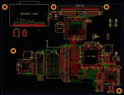
A possibly idealized layout would have the CPLD in between the MPU and the rest of the address and data bus end points (EPROM, RAM, etc.). There isn't enough space on the board to allow such a layout. Another possibility is for the CPLD to be angularly displaced relative to the MPU. The attached illustration, which is a work in progress, has such a layout.

Attachment:
File comment: POC V3 PCB Work-in-Progress
pocv3pcb.jpg
pocv3pcb.jpg [ 2.76 MiB | Viewed 819 times ]

This layout, which is on a truncated micro-ATX PCB, includes Garth's 4MB DIMM, which is to the left of the CPLD, which in turn, is at the top left corner of the MPU. Also, bus drivers/transceivers are part of the design, as the potential bus loading is much higher than my earlier efforts. They are located around the MPU to keep the latter's connections reasonably short.

As for the MAX-238s, their connections operate at the relatively low speed of the TIA-232 signaling rate, no more than 230.4 Kbps in my application. Positioning is non-critical. An alternative that I have considered in place of the two MAX-238s is a single MAX-248, which is essentially four MAX-232s in a PLCC-44 package. However, the single-piece price of the MAX-248 is some 23 USD, versus 15 USD for two MAX-238s. Paying an extra 8 USD to slightly compact the layout seems counterproductive for a hobby computer, no?

I'm always amenable to suggestions, which is why I post this stuff for commentary. Sometimes I don't always see the forest, only a bunch of trees.

Attachment:
File comment: MAX2xx Series TIA-232 Transceivers
LINEDRIVER_max220_max249.pdf [371.61 KiB]
Downloaded 61 times

_________________
x86?  We ain't got no x86.  We don't NEED no stinking x86!


Top
 Profile  
Reply with quote  
 Post subject: Re: POC Version 2
PostPosted: Thu Feb 27, 2014 8:02 pm 
Offline
User avatar

Joined: Fri Aug 30, 2002 1:09 am
Posts: 8430
Location: Southern California
Quote:
Paying an extra 8 USD to slightly compact the layout seems counterproductive for a hobby computer, no?

I figure that if I'm only making one, my value of time in design and assembly is well beyond that of the parts, which is why I have a bunch of WW PLCC sockets here which I paid about $10 each for. The price of multilayer PCBs OTOH is intimidating. I design them frequently for work, but we never order less than a hundred at a time, so the set-up charges (some amortized and some not) become quite acceptable.

_________________
http://WilsonMinesCo.com/ lots of 6502 resources
The "second front page" is http://wilsonminesco.com/links.html .
What's an additional VIA among friends, anyhow?


Top
 Profile  
Reply with quote  
 Post subject: Re: POC Version 2
PostPosted: Fri Feb 28, 2014 7:34 am 
Offline
User avatar

Joined: Thu May 28, 2009 9:46 pm
Posts: 8172
Location: Midwestern USA
GARTHWILSON wrote:
Quote:
Paying an extra 8 USD to slightly compact the layout seems counterproductive for a hobby computer, no?

I figure that if I'm only making one, my value of time in design and assembly is well beyond that of the parts, which is why I have a bunch of WW PLCC sockets here which I paid about $10 each for. The price of multilayer PCBs OTOH is intimidating. I design them frequently for work, but we never order less than a hundred at a time, so the set-up charges (some amortized and some not) become quite acceptable.

In the case of POC V2, the theoretically more compact layout that would be achieved with the MAX-248 is not of any particular value. The PCB cost is fixed regardless of size and number of holes, assuming the 21 square inch/650 hole limit of ExpressPCB's Proto-Pro service is not exceeded. On the other hand, if I were going to build one hundred copies of this unit, I'd be using a production PCB service, and board size and hole count would become important.

My general approach has been to concentrate time on compacting areas where compaction will achieve something of value. As I mentioned, the MAX-238 connections are relatively low speed. So issues that would arise with, say, overly-long address connections aren't likely to occur.

_________________
x86?  We ain't got no x86.  We don't NEED no stinking x86!


Top
 Profile  
Reply with quote  
 Post subject: Re: POC Version 2
PostPosted: Mon Mar 24, 2014 12:13 am 
Offline
User avatar

Joined: Thu May 28, 2009 9:46 pm
Posts: 8172
Location: Midwestern USA
BigDumbDinosaur wrote:
In the case of POC V2, the theoretically more compact layout that would be achieved with the MAX-248 is not of any particular value...

Just for grins, I decided to take another look at using the MAX248 in place of two MAX238s. Attached are the revised schematic (pages 4, 5 and 6) and the revised PCB layout. Compare this new PCB layout with the one above and you will see that the MAX248, along with its charge pump capacitors, takes up less space than the two MAX238s, even though the latter are SOIC devices. Dunno if I'm convinced, though, to spend the extra money just so I have more unused board space. :lol:

On the plus side, soldering a PLCC44 socket into the board is easier than soldering two 24 pin SOIC devices. Hmm...

Attachment:
File comment: POC V2.0 Schematic w/MAX248, Page 4
poc_v2_p4.gif
poc_v2_p4.gif [ 130.92 KiB | Viewed 755 times ]
Attachment:
File comment: POC V2.0 Schematic w/MAX248, Page 5
poc_v2_p5.gif
poc_v2_p5.gif [ 132.22 KiB | Viewed 755 times ]
Attachment:
File comment: POC V2.0 Schematic w/MAX248, Page 6
poc_v2_p6.gif
poc_v2_p6.gif [ 121.15 KiB | Viewed 755 times ]
Attachment:
File comment: POC V2.0 PCB Layout w/MAX248
poc_v2pcb.jpg
poc_v2pcb.jpg [ 1.65 MiB | Viewed 755 times ]

_________________
x86?  We ain't got no x86.  We don't NEED no stinking x86!


Top
 Profile  
Reply with quote  
Display posts from previous:  Sort by  
Post new topic Reply to topic  [ 544 posts ]  Go to page Previous  1 ... 9, 10, 11, 12, 13, 14, 15 ... 37  Next

All times are UTC


Who is online

Users browsing this forum: No registered users and 13 guests


You cannot post new topics in this forum
You cannot reply to topics in this forum
You cannot edit your posts in this forum
You cannot delete your posts in this forum
You cannot post attachments in this forum

Search for:
Jump to: