6502.org Forum  Projects  Code  Documents  Tools  Forum
It is currently Sun May 05, 2024 8:35 am

All times are UTC


Post new topic Reply to topic  [ 564 posts ]  Go to page Previous  1 ... 27, 28, 29, 30, 31, 32, 33 ... 38  Next
Author Message
PostPosted: Thu May 20, 2021 1:34 am 
Offline
User avatar

Joined: Tue Mar 05, 2013 4:31 am
Posts: 1373
Well, hate to say it, but a dead SBC "should" be easier to troubleshoot than an intermittent one. I also would not suspect a VIA problem, but you never know. I found a bad VIA last year while repairing an old Vic-20... the bad VIA was just under the CPU socket... a bit tricky to find.... but I just took the approach of ringing out all of the address lines and data lines first... from/to everywhere they go and ensure a continuity check but also of low resistance.

Like you, I would tend to suspect the RAM going south on you, due to the suspect nature of putting a bit of pressure on it. Chances are it has an internal fracture of one or more connections.... or the SRAM itself became contaminated from a manufacturing problem. An old friend of mine also joined IBM shortly after I did.... he worked in the semi lab doing chip failure analysis... the stuff he found over the decades was quite interesting. After a while, other major chip manufacturers were sending their failed parts for analysis as they couldn't locate the cause... my buddy always did (find the cause).

In any case, I'd likely start by replacing the SRAM... hopefully it may be a quicker exercise than metering out the entire PCB. On the shotgun approach... just replace everything that's socketed.... you never know. Do let us know what you find.... logic probes... when you need one, there's never one in sight!

_________________
Regards, KM
https://github.com/floobydust


Top
 Profile  
Reply with quote  
PostPosted: Thu May 20, 2021 2:02 am 
Offline
User avatar

Joined: Fri Aug 30, 2002 1:09 am
Posts: 8432
Location: Southern California
floobydust wrote:
On the shotgun approach... just replace everything that's socketed.... you never know.

The only problem I've had with my workbench computer in 28 years was socket connections; and pulling the ICs up a bit and pushing them back down in for some self-cleaning effect on the contacts brought it back. This kind of thing is why military electronics don't allow sockets. ICs must be soldered in, or so I hear anyway. (The only exception to the sockets problem was when I accidentally let an all-metal screwdriver roll under it when it was powered up and it shorted WW pins together. I never bothered to see which ICs were damaged. I just replaced them all.)

_________________
http://WilsonMinesCo.com/ lots of 6502 resources
The "second front page" is http://wilsonminesco.com/links.html .
What's an additional VIA among friends, anyhow?


Top
 Profile  
Reply with quote  
PostPosted: Thu May 20, 2021 5:10 am 
Offline
User avatar

Joined: Thu May 28, 2009 9:46 pm
Posts: 8173
Location: Midwestern USA
floobydust wrote:
Well, hate to say it, but a dead SBC "should" be easier to troubleshoot than an intermittent one.

In this case, it should be easier, since the unit was working. It would be harder to fix if it had not worked at all.

Quote:
Like you, I would tend to suspect the RAM going south on you, due to the suspect nature of putting a bit of pressure on it...In any case, I'd likely start by replacing the SRAM...

Replacing the RAM is easier said than done—it's an SOJ package. I can desolder it without any problem by using my small heat gun. The problem is in installing the new one. I used to be able to solder SOJ packages—I built V1.0 and two copies of V1.1 with manually soldering the SRAM, but that was back when I could see.

In any case, the first step would be to determine if the SRAM is the source of the trouble.

Quote:
...On the shotgun approach... just replace everything that's socketed.... you never know.

I had already tried replacing the MPU with one I know works when this problem first arose, with no change. Here's what I have discovered so far.

There is activity on the 65C816's VPA pin immediately after reset, which means the MPU is fetching instructions. Since that is lasting more that a fraction of a second, it suggests the first stage POST, in which physical zero page, the emulation mode stack and kernel workspace are tested, was completed. If there had been a RAM error the MPU should have halted after executing a STP instruction...which didn't happen.

I'm stumped at the moment. The MPU is doing something, but it doesn't appear to be doing anything useful. The thing with SRAM is it powers up with random garbage in it and to the 65C816, it all looks like code, since there are no invalid opcodes.

Knowing that the MPU is good (it runs in POC V1.1 at 14 MHz) and is doing something, the next step will be to pull the Ø2 oscillator and replace it with the single-stepper. Along with that, I will hook up the logic analyzer and see what is showing up on the address bus at the beginning of the stage one POST. That code runs out of ROM, so I should be seeing a ROM address on the address bus when VPA is high. I've got plenty of inputs on the logic analyzer, so I should also be able to monitor the data bus to see what is showing up on it during the opcode and operand fetch cycles.

Stay tuned...

_________________
x86?  We ain't got no x86.  We don't NEED no stinking x86!


Last edited by BigDumbDinosaur on Thu May 20, 2021 8:07 am, edited 1 time in total.

Top
 Profile  
Reply with quote  
PostPosted: Thu May 20, 2021 6:45 am 
Offline

Joined: Sun Jun 29, 2014 5:42 am
Posts: 337
BigDumbDinosaur wrote:
[color=#000000]
I've got plenty of inputs on the logic analyzer, so I should also be able to monitor the data bus to see what is showing up on it during the opcode and operand fetch cycles.

Can your logic analyzer do synchronous capture on the falling edge of the clock? (i.e. one sample per clock edge)

If you connect it as follows and take a trace of the boot sequence, we can run in through the open source 6502/65816 decoder:
- bit 14: nRST
- bit 12: E
- bit 11: VPA
- bit 10: RDY
- bit 9: VPD
- bit 8: RnW
- bit 7..0: DATA

The 6502/65816 decoder is a standalone tool for interpretting logic analuzer capture files. It works like the "inverse assembler" feature of the old HP logici analyzers. It will give you a full instruction trace of the reset sequence, together with full modelling of the registers and memory. If there is a memory fault it will flag it directly.

We've used it very successfully to debug Beeb816, and also to debug Drass's excellent 65816 test suite.

I'd be happy to help here if you can capture the data.

Dave


Top
 Profile  
Reply with quote  
PostPosted: Thu May 20, 2021 8:10 am 
Offline
User avatar

Joined: Thu May 28, 2009 9:46 pm
Posts: 8173
Location: Midwestern USA
hoglet wrote:
BigDumbDinosaur wrote:
I've got plenty of inputs on the logic analyzer, so I should also be able to monitor the data bus to see what is showing up on it during the opcode and operand fetch cycles.

Can your logic analyzer do synchronous capture on the falling edge of the clock? (i.e. one sample per clock edge)

I believe it can.

Quote:
If you connect it as follows and take a trace of the boot sequence, we can run in through the open source 6502/65816 decoder...I'd be happy to help here if you can capture the data.

Dave

Thanks for the offer. I should be able to do a capture if I truly get stuck and can't figure it out.

_________________
x86?  We ain't got no x86.  We don't NEED no stinking x86!


Top
 Profile  
Reply with quote  
PostPosted: Thu May 20, 2021 2:26 pm 
Offline

Joined: Fri Dec 21, 2018 1:05 am
Posts: 1076
Location: Albuquerque NM USA
BDD,
I'm pretty good with fine pitch soldering down to 0.5mm pitch SMT and I have a hot air tool to remove SOJ. I live in New Mexico. I'm happy to replace your RAM and help you build up SMT portion of 2nd board free of charge.
Bill


Top
 Profile  
Reply with quote  
PostPosted: Thu May 20, 2021 6:34 pm 
Offline
User avatar

Joined: Thu May 28, 2009 9:46 pm
Posts: 8173
Location: Midwestern USA
plasmo wrote:
BDD,
I'm pretty good with fine pitch soldering down to 0.5mm pitch SMT and I have a hot air tool to remove SOJ. I live in New Mexico. I'm happy to replace your RAM and help you build up SMT portion of 2nd board free of charge.
Bill

Thanks for the offer.

I'm not at the point where I can conclusively condemn the SRAM and after working on this problem some more last night, I temporarily set it aside so I could work on something else that had been languishing since last year.

POC V1.2 was a "bridge" design intended to test four-channel serial I/O via two DUARTs, serial I/O interrupt steering, and wait-stating via clock-stretching. All these concepts have been successfully implemented in V1.2, so the unit has served its purpose. That an apparent mechanical issue caused it to go belly-up isn't real concerning to me, since I know the circuit is functional at 20 MHz. At some point, the problem will get solved.

_________________
x86?  We ain't got no x86.  We don't NEED no stinking x86!


Top
 Profile  
Reply with quote  
PostPosted: Sun May 23, 2021 6:56 am 
Offline
User avatar

Joined: Thu May 28, 2009 9:46 pm
Posts: 8173
Location: Midwestern USA
BigDumbDinosaur wrote:
plasmo wrote:
BDD,
I'm pretty good with fine pitch soldering down to 0.5mm pitch SMT and I have a hot air tool to remove SOJ. I live in New Mexico. I'm happy to replace your RAM and help you build up SMT portion of 2nd board free of charge.
Bill

Thanks for the offer.

I'm not at the point where I can conclusively condemn the SRAM and after working on this problem some more last night, I temporarily set it aside so I could work on something else that had been languishing since last year.

As I had said, I decided to save the POC V1.2 failure diagnosis for another day. Being mechanical in nature, I'm not going to make it a priority. I know the circuit is functional.

Last year, I had started development of a new unit in the POC V1 series, one that would have the features of V1.2, but also would make use of the upper half of the 128KB SRAM with which all my POC units have been equipped—POC V1.0 and V1.1 have 52KB of addressable RAM, and V1.2 has 48KB.

As things went, I couldn't devote much time to hobby computing for a while and the new design gathered dust. Things have improved since then and the machine is done and runs.

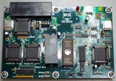
Ladies and gentlemen, meet POC V1.3.

Attachment:
File comment: POC V1.3 Top View
poc_v1.3_top.jpg
poc_v1.3_top.jpg [ 1.76 MiB | Viewed 72375 times ]

V1.3 is basically the V1.2 circuit, but with a stretchable clock generation circuit for wait-stating ROM and I/O accesses, and a latch to generate A16, thus giving access to almost all of the SRAM. The range $00C000-$00FFFF is I/O and ROM—the rest is RAM. That arrangement works out to 112KB of addressable RAM, of which about 110KB is available for user code and data—the firmware "owns" the remaining 2KB. The entire $010000-$01FFFF range is available for user code and data.

Like its predecessors, V1.3 is entirely discrete logic and all but one piece of it is SMT. There is slightly more propagation delay in the logic due to the generation of a signal that indicates when a bank $00 access is occurring—the purpose being to avoid having I/O and ROM mirrored above $00FFFF. The method I used to generate that signal is not super-efficient. However, it does the job—V1.3 worked properly on the first try.

Initial boot-up was using V1.2's ROM, which of course didn't know about the extra RAM now available. Once I saw a successful POST, I modified the firmware to do a non-destructive RAM test above $00FFFF and report the results. Here's the POST screen for the new machine:

Attachment:
File comment: POC V1.3 POST Display
poc_v1.3_post.jpg
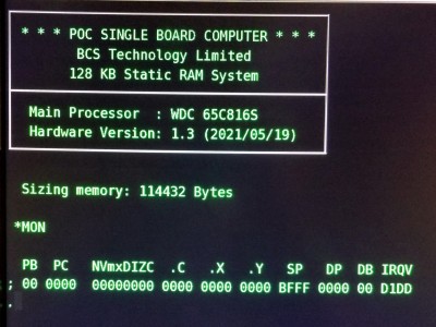
poc_v1.3_post.jpg [ 1.85 MiB | Viewed 72375 times ]

Here's the schematic:

Attachment:
File comment: POC V1.3 Schematic
pocv130.pdf [344.54 KiB]
Downloaded 135 times

What follows are some detail photos of the unit.

Attachment:
File comment: POC V1.3 Panic Buttons
poc_v1.3_detail03.jpg
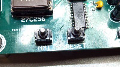
poc_v1.3_detail03.jpg [ 1.43 MiB | Viewed 72375 times ]

Seen in the above photo are NMI and reset push buttons mounted on the board for those times when some boneheaded programming causes the unit to get stuck in the mud, or go off the road and smack into a tree.

Attachment:
File comment: POC V1.3 Power Connector & Status Indicators
poc_v1.3_detail04.jpg
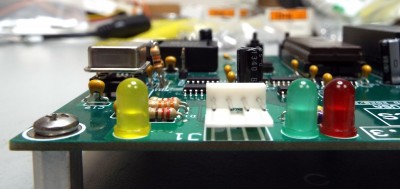
poc_v1.3_detail04.jpg [ 994.93 KiB | Viewed 72375 times ]

Seen in the above photo (left to right) are the yellow IRQ "heartbeat" indicator, a feature introduced in V1.2 (but with the LED correctly hooked up this time), power input connector (3.5" floppy disk Berg connector), green "power good" indicator, and red reset indicator.

Attachment:
File comment: POC V1.3 Serial I/O Hardware
poc_v1.3_detail02.jpg
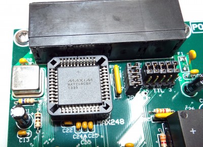
poc_v1.3_detail02.jpg [ 1.96 MiB | Viewed 72375 times ]

Like V1.2, V1.3 has four, high-speed TIA-232 ports, with a pair of NXP 28L92 DUARTs acting as a virtual QUART—the driver is the same as in V1.2. A change I made to the serial I/O circuit was to replace the two MAX238 transceivers used in V1.2 with a single MAX248. Although the combination of a single MAX248 and its socket (PLCC44) costs slightly more than a pair of MAX238s in SOIC, the MAX248 requires only four charge-pump capacitors to handle all four channels, whereas the MAX238 pair required eight total. Also, I can easily solder a PLCC44 socket, as the pins are on a 100×100 mil grid. Soldering anything SMT has become very difficult for me.

Attachment:
File comment: POC V1.3 Clock Generation
poc_v1.3_detail01.jpg
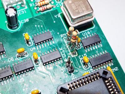
poc_v1.3_detail01.jpg [ 2.12 MiB | Viewed 72375 times ]

Above is the clock generation hardware.

Due to the use of a 74AC573 latch to generate A16, both Ø1 and Ø2 clocks are needed. The clock circuit in V1.3 uses a 74AC74 C-D flop to generate the signals, and a 74AC109 J-K flop to wait-state ROM and I/O accesses. A wait-state is produced by stretching the Ø2 high phase an additional cycle, with a corresponding stretch of the Ø1 low phase, a principle which I wrote about here. The AC109 acts as a timer to stop the clock for one Ø2 cycle, using a circuit illustrated by Jeff.

As both clocks come from the same AC74 flop, they are exactly (within a fraction of a nanosecond) 180 degrees out of phase. Therefore, the 573 latch closes within a few nanoseconds of the rise of Ø2. This mess works fine at 16 MHz, but is unstable at 20 MHz. As soon as time permits, I will hook up the logic analyzer and have a gander at the timing.

Oh, about those two resistors sticking up by the clock oscillator... :D

Originally, there was a two-resistor SIP at that location (RN1 in the schematic), the resistors' purpose being to dampen ringing on the clock signals. During testing to check for clock signals, voltages being present, etc., I was dismayed to discover the Ø1 and Ø2 signals coming out of the SIP were distorted, with slow edges and rounded corners. The signals were okay on the "upstream" side of the SIP, which led to me concluding the SIP had too much capacitance and was munging up the signals. So I removed it and scabbed in some 100 ohm carbon film resistors from my parts supply. Now I had proper-looking clock signals.

Hmm...

_________________
x86?  We ain't got no x86.  We don't NEED no stinking x86!


Last edited by BigDumbDinosaur on Sun May 30, 2021 4:54 am, edited 1 time in total.

Top
 Profile  
Reply with quote  
PostPosted: Mon May 24, 2021 12:07 pm 
Offline
User avatar

Joined: Tue Mar 05, 2013 4:31 am
Posts: 1373
Wow, very nice to see 1.3 up and running. Lots of SMT on the new version as well. I grabbed the schematic, very nice. Kinda surprised that you avoided using a (C)PLD or two for much of the glue logic, but you can't argue with success.

As an aside... looks like you used PCBexpress for the schematic... if yes, did you also use them for making the PCB?

_________________
Regards, KM
https://github.com/floobydust


Top
 Profile  
Reply with quote  
PostPosted: Mon May 24, 2021 2:03 pm 
Offline
User avatar

Joined: Fri Dec 11, 2009 3:50 pm
Posts: 3351
Location: Ontario, Canada
Congratulations on the new addition to your "family"! Version 1.3 looks great. :)

I have doubts about your theory regarding the SIP resistors, though. It's not plausible that they'd have too much capacitance -- that value would on the order of a few picofarads, easily manhandled by the 74AC74 that's driving them.

Is it possible the SIP that was in there had a different resistance than intended (ie, higher)? The lettering on those parts is awfully tiny, and I know your eyesight isn't the best...

-- Jeff

_________________
In 1988 my 65C02 got six new registers and 44 new full-speed instructions!
https://laughtonelectronics.com/Arcana/ ... mmary.html


Top
 Profile  
Reply with quote  
PostPosted: Mon May 24, 2021 8:22 pm 
Offline
User avatar

Joined: Thu May 28, 2009 9:46 pm
Posts: 8173
Location: Midwestern USA
floobydust wrote:
Wow, very nice to see 1.3 up and running. Lots of SMT on the new version as well. I grabbed the schematic, very nice. Kinda surprised that you avoided using a (C)PLD or two for much of the glue logic, but you can't argue with success.

V1.3 was an incremental design and since the glue logic from V1.2 (which I had running at 20 MHz) would work with a minor change to accommodate the extra RAM, I figured why not use it. V1.3 has one more chip than V1.2—it gained two chips with the addition of the bank latch and the J-K flop, but lost a chip with the switch from two MAX238s to one MAX248.

With V1.2, I had "standardized" on a new board shape and size (the old shape and size was dictated by ExpressPCB's "Proto-Pro" size limits), and when I did the layout in DIP it got to be a bit too much like the interior of Noah's ark after all the animals had boarded. :D Hence the proliferation of SMT parts.

I have one more design iteration in the V1.x series I'd like to try and that is building a unit with 512KB of RAM. The circuit would be almost the same as V1.3's but with a little more complication in generating the bank $00 signal that prevents I/O and ROM mirroring above $00FFFF. That unit would be V1.4 and would be the final design of the series.

While it is possible to go beyond 512KB in discrete logic, the circuit would get unwieldy with having to manage multiple RAM chip selects. That's a job for a CPLD.

Quote:
As an aside... looks like you used PCBexpress for the schematic... if yes, did you also use them for making the PCB?

I think you meant ExpressPCB (different company). I did use their schematic and PCB layout software but then converted the PCB layout to Gerbers and had the boards made at JLCPCB. The latter is considerably cheaper and the product quality is as good as that of ExpressPCB (who don't actually make their boards).

Dr Jefyll wrote:
Congratulations on the new addition to your "family"! Version 1.3 looks great. :)

Thanks! Best part (so far) is no bodge wiring was needed. :D

Quote:
I have doubts about your theory regarding the SIP resistors, though. It's not plausible that they'd have too much capacitance -- that value would on the order of a few picofarads, easily manhandled by the 74AC74 that's driving them.

Is it possible the SIP that was in there had a different resistance than intended (ie, higher)? The lettering on those parts is awfully tiny, and I know your eyesight isn't the best...

I did meter the SIP after I removed it and it was 102 ohms, well within tolerance. As you say, the lettering is microscopic and I've definitely developed Mr. Magoo symptoms. So there was the possibility I had stuck the wrong value in there. More likely than not, I managed to get a defective part...it happens now and then.

Since V1.3 is running stable at 16 MHz and I have a few more of those 100 ohm SIPs, I may try pulling out the resistors and scabbing a SIP in there to see what happens. The little surprise with the clock signals was why I went "Hmm..." at the end of my previous post. I've never had any reason to suspect a SIP resistor array would do anything dastardly to a clock signal.

_________________
x86?  We ain't got no x86.  We don't NEED no stinking x86!


Top
 Profile  
Reply with quote  
PostPosted: Tue May 25, 2021 2:33 am 
Offline
User avatar

Joined: Tue Mar 05, 2013 4:31 am
Posts: 1373
Yes, my keyboard dyslexia setting in... ExpressPCB is what I'm using as well. I've also got a fair number of custom PCB components and schematic parts I've created, so I really don't feel like changing to another tool for schematics and PCBs... their price is on the high side, but they do offer gerbers now when ordering. I recall you having some software that will convert their format to gerbers... does it also handle their 4-layer and newer 6-layer formats?

I'm starting work on the C02 Pocket SBC 3... single PCB in the same 2.5" x 3.8" format that will combine the two PCBs I'm using now (C02 Pocket SBC and RTC/CF-Card Adapter) and be mostly SMT components... likely 3.3V as well. Anyway... back to POC V1.3...

Are you also able to use your previous SCSI adapter on V1.3? I'm thinking your POC should have ample power to manage it's own filesystem and run a full dev environment with the proper storage subsystem, which would be nice.

_________________
Regards, KM
https://github.com/floobydust


Top
 Profile  
Reply with quote  
PostPosted: Tue May 25, 2021 2:46 am 
Offline
User avatar

Joined: Thu May 28, 2009 9:46 pm
Posts: 8173
Location: Midwestern USA
floobydust wrote:
I recall you having some software that will convert their format to gerbers... does it also handle their 4-layer and newer 6-layer formats?

The conversion software predates the six-layer format, so it may not be able to understand it. If you have a 6-layer design you want to send me via PM I can try it.

Quote:
Are you also able to use your previous SCSI adapter on V1.3?

It's electrically compatible but not mechanically. I have a "new and improved" host adapter on the drawing board, that aside from fitting the footprint of V1.3 (and V1.2), has some features I omitted in the original design (which dates from 2011).

_________________
x86?  We ain't got no x86.  We don't NEED no stinking x86!


Last edited by BigDumbDinosaur on Mon Nov 15, 2021 12:31 am, edited 1 time in total.

Top
 Profile  
Reply with quote  
PostPosted: Mon May 31, 2021 6:16 pm 
Offline
User avatar

Joined: Thu May 28, 2009 9:46 pm
Posts: 8173
Location: Midwestern USA
Okay, discovered an interesting anomaly in POC V1.3.

Using MVN or MVP to copy data from bank $01 to bank $00 works like a charm. Using either instruction to copy data from bank $00 to bank $01 crashes the machine. Using either instruction to copy data from one place in bank $01 to another in bank $01 also causes the machine to croak. No such problem occurs if activity is confined to bank $00.

It's not a clock speed issue: the problem occurs at any speed I test, 1 MHz being the slowest. :roll: :!: :shock:

_________________
x86?  We ain't got no x86.  We don't NEED no stinking x86!


Top
 Profile  
Reply with quote  
PostPosted: Tue Jun 01, 2021 12:18 am 
Offline
User avatar

Joined: Tue Mar 05, 2013 4:31 am
Posts: 1373
BigDumbDinosaur wrote:
Okay, discovered an interesting anomaly in POC V1.3.

Using MVN or MVP to copy data from bank $01 to bank $00 works like a charm. Using either instruction to copy data from bank $00 to bank $01 crashes the machine. Using either instruction to copy data from one place in bank $01 to another in bank $01 also causes the machine to croak. No such problem occurs if activity is confined to bank $00.

It's not a clock speed issue: the problem occurs at any speed I test, 1 MHz being the slowest. :roll: :!: :shock:


That can't be fun to find out after the fact.... so, not being that familiar with the 65C816, dare I suggest using a normal memory move routine between banks? No idea if it would behave differently, but if it did work, then perhaps you've found a hardware timing anomaly with the bank logic.... I'm really guessing here.

_________________
Regards, KM
https://github.com/floobydust


Top
 Profile  
Reply with quote  
Display posts from previous:  Sort by  
Post new topic Reply to topic  [ 564 posts ]  Go to page Previous  1 ... 27, 28, 29, 30, 31, 32, 33 ... 38  Next

All times are UTC


Who is online

Users browsing this forum: Sittingbull and 14 guests


You cannot post new topics in this forum
You cannot reply to topics in this forum
You cannot edit your posts in this forum
You cannot delete your posts in this forum
You cannot post attachments in this forum

Search for:
Jump to: