6502.org Forum  Projects  Code  Documents  Tools  Forum
It is currently Thu May 09, 2024 8:40 pm

All times are UTC


Post new topic Reply to topic  [ 564 posts ]  Go to page Previous  1 ... 32, 33, 34, 35, 36, 37, 38  Next
Author Message
PostPosted: Tue Mar 29, 2022 2:21 pm 
Offline
User avatar

Joined: Sun Jun 30, 2013 10:26 pm
Posts: 1928
Location: Sacramento, CA, USA
How did you discover the collision? Was it a mysterious crash? Have you considered the idea of checking your SP value once every "jiffy" and triggering a "kernel panic" if it crosses below a certain threshold?

_________________
Got a kilobyte lying fallow in your 65xx's memory map? Sprinkle some VTL02C on it and see how it grows on you!

Mike B. (about me) (learning how to github)


Top
 Profile  
Reply with quote  
PostPosted: Tue Mar 29, 2022 6:45 pm 
Offline
User avatar

Joined: Thu May 28, 2009 9:46 pm
Posts: 8178
Location: Midwestern USA
barrym95838 wrote:
How did you discover the collision? Was it a mysterious crash?

What alerted me was some output to serial I/O channel D would periodically get corrupted. When an IRQ occurred during the middle of a deeply-nested function call, the stack space “requisitioned” by the IRQ would impinge by a couple of bytes into the tail end of channel D’s transmit queue. If the queue pointer happened to be pointing to that part of the queue at the time, the port would output gibberish. It took about an hour’s worth of troubleshooting to figure out what was going on.

Quote:
Have you considered the idea of checking your SP value once every "jiffy" and triggering a "kernel panic" if it crosses below a certain threshold?

I have, but the relocation of the top-of-stack makes it less a problem than it was. On the other hand, accidentally pointing the stack too high would be destructive and could be something to watch for.

_________________
x86?  We ain't got no x86.  We don't NEED no stinking x86!


Top
 Profile  
Reply with quote  
PostPosted: Sat Apr 30, 2022 8:37 pm 
Offline
User avatar

Joined: Thu May 28, 2009 9:46 pm
Posts: 8178
Location: Midwestern USA
About a week ago, I went to use the logic probe to look at something on POC V1.3, only to have the entire mess suddenly go dead, meaning “dead” as in “there isn’t any power” dead. I turned off the mains switch on the power supply, waited a few seconds and tried powering up. Nothing! I tried it again, same result (yes, I know: insanity is repeating some action and expecting a different result each time). I had unpleasant visions of something on the POC unit having been somehow destroyed by me poking it with the probe. It wouldn’t be the first time!

By way of explanation, I should mention that the POC unit and its disks are run by an ancient power supply that I scabbed from an equally-ancient PC from the 1990s. Since the power supply is very old, not only was I having unpleasant visions of toasted POC parts, the possibility the power supply had decided to pack it in was swirling in my mind.

First thing I did was disconnect POC and the disks so nothing would get anymore damaged than I already thought it was. Since PC power supplies usually require a minimum amount of loading to power up, I plugged in a makeshift artificial load (a 10 ohm, wirewound resistor with an LED in parallel for a visual indication of power) on one of the unused Molex connectors and flipped the switch. The power supply very briefly produced power, evidenced by the LED flashing, and then died. Okay, it appeared the power supply may have breathed its final breath. Not a problem—I've got more power supplies scavenged from old machines.

While I was contemplating the situation, I saw something that explained the sudden “failure.”

Attachment:
rats_nest01.gif
rats_nest01.gif [ 1.16 MiB | Viewed 167606 times ]

Above is the POC “test rig,” which may be charitably described as a rat’s nest of wires and cables. The logic probe gets its power from a crude connection consisting of an old Molex connector chopped off a power supply extender harness, with two wires stripped to provide five volts and ground. Hey, I was eager to get the computer running—beautifying the installation was a project for another time. :D

Attachment:
rats_nest02.gif
rats_nest02.gif [ 1.1 MiB | Viewed 167606 times ]

Above is how the logic probe is powered.

At this point, I’m sure you can surmise what had happened. I picked up the probe to use it and somehow the two bare connections got together, said “Let’s give him a scare.” and proceeded to short out the power supply. The power supply did what it is supposed to do, which is immediately shut down. I, of course, thought I had managed to hit two pins at the same time on the chip I was probing and thus managed to brick the chip...and the computer. Since the short remained after I had disconnected everything except the logic probe, testing the power supply made it appear that it had coughed its cookies.

Once I had separated the errant wires and reconnected everything, V1.3 powered up and all was well. Ah, the perils of monkey-rigged wiring!

Incidentally, that thing on which the logic probe is resting in the first photo is a VGA-to-USB converter, whose input is driven by a VGA splitter, which in turn, is connected to the thin client that acts as POC’s console. With that, I am now able to capture POC’s video output in real time on my creaky, old Windows XP workstation. I got the parts from an Amazon vendor—they work like a charm.

_________________
x86?  We ain't got no x86.  We don't NEED no stinking x86!


Top
 Profile  
Reply with quote  
 Post subject: POC Computer Version One
PostPosted: Mon Jun 13, 2022 7:43 am 
Offline
User avatar

Joined: Thu May 28, 2009 9:46 pm
Posts: 8178
Location: Midwestern USA
POC V1.3 keeps chugging along as I debug my filesystem software. Here’s an uptime snapshot.

Attachment:
File comment: POC V1.3 Uptime
uptime_20220613.png
uptime_20220613.png [ 346.54 KiB | Viewed 167537 times ]

_________________
x86?  We ain't got no x86.  We don't NEED no stinking x86!


Top
 Profile  
Reply with quote  
PostPosted: Sat Jul 30, 2022 10:11 pm 
Offline
User avatar

Joined: Thu May 28, 2009 9:46 pm
Posts: 8178
Location: Midwestern USA
POC V1.3 has been officially “put to bed.” It served its purpose, which was primarily to look at how everything behaves when the bank latch gets involved. V1.3 demonstrated that bank latching in discrete logic is practical at double-digit Ø2 rates. Also, V1.3 proved my stretchable clock circuit is reliable up to at least 16 MHz. V1.3 is the final version of POC units using discrete logic. I don't contemplate building a POC V1.4, although I did have a design on the “drawing board” at one time.

Speaking of which, something I'd like to explore is rigging up a simple network between two or more POC units via TIA-485. The 28L92 DUART can do up to 921 KbPS using the built-in bit rate generator and with the use of a suitable transceiver, can communicate with TIA-485, asynchronously or synchronously. Even higher speeds are possible by using an external clock source to set the bit rate. At 921 KbPS, permissible bus length is around 105 meters (354 feet), assuming use of UTP cable and proper termination. Effective throughput would be about 90 KB/second, which is fast enough to process data in short to medium bursts.

It’s only a thought...for now...

_________________
x86?  We ain't got no x86.  We don't NEED no stinking x86!


Top
 Profile  
Reply with quote  
PostPosted: Sat Jul 30, 2022 10:28 pm 
Offline
User avatar

Joined: Fri Aug 30, 2002 1:09 am
Posts: 8432
Location: Southern California
BigDumbDinosaur wrote:
something I'd like to explore is rigging up a simple network between two or more POC units via TIA-485.

Do you have any favorite 485 line drivers and receivers (or any you have your eye on to use)?

_________________
http://WilsonMinesCo.com/ lots of 6502 resources
The "second front page" is http://wilsonminesco.com/links.html .
What's an additional VIA among friends, anyhow?


Top
 Profile  
Reply with quote  
PostPosted: Sun Jul 31, 2022 6:13 am 
Offline
User avatar

Joined: Thu May 28, 2009 9:46 pm
Posts: 8178
Location: Midwestern USA
GARTHWILSON wrote:
BigDumbDinosaur wrote:
something I'd like to explore is rigging up a simple network between two or more POC units via TIA-485.

Do you have any favorite 485 line drivers and receivers (or any you have your eye on to use)?

I'm partial to Maxim’s MAX485 (data sheet attached). Only thing needed with it is a termination setup, which can be fashioned from three carbon-film or metal-film resistors and a jumper block to enable or disable termination as needed

For the benefit of readers who aren't familiar with TIA-485, it is a communications layer arranged as a multidrop bus, sort of like SCSI. TIA-485 uses differential signaling and is able to reliably operate at distances up to 4000 feet (1219 meters). Maximum speed is 10 Mb/sec over short distances. Speeds of 1 Mb/sec are practical over a distance of 354 feet (105 meters). TIA-485 only defines the electrical characteristics—data transmission protocol is not part of the standard, nor are details such as cable type, method of connection between cable and device, etc. All TIA-485 defines are voltage levels and bus arrangement, which is very simple.

Each connected device is a “station” and all stations are wired to the bus in daisy-chain fashion. The end stations have the bus terminated to suppress signal reflections. There is no theoretical limit to the number of stations that can be connected that I know of. Cabling is either UTP or shielded, UTP usually being the preference because it’s cheap and easy to install (when I was doing such installations I was wiring to T568B standards, same as 10/100/1000Base-T Ethernet). In a factory environment, it’s common to run the cable in grounded EMT to protect it from physical damage and strong electromagnetic fields.

As TIA-485 is a bus topology, it is normally not rigged up in a star configuration like Ethernet is when using UTP cable. Many installations are half-duplex, but making a TIA-485 network full duplex is a simple matter; one more wire pair and another transceiver per station is required.

Bus connections to stations can be made by almost any means—I’ve seen screw terminals, D-subs, 4, 6 and 8 position modular jacks (8P8C, often incorrectly referred to as RJ45, is common) and even old-fashioned Jones plugs. On one occasion, I monkey-rigged a bus connection by twisting some wires together because a maintenance guy in the client’s plant got ham-fisted and busted the DB-25 connector on the back of the machine’s control panel. They ran with it for several years. :shock:

Incidentally, the old Apple Talk network that linked up Macs in school computer labs ran on TIA-422, which is a slightly dumbed-down version of TIA-485.

Attachment:
File comment: Maxim TIA422/485 Transceivers
linedriver_rs485_max1487_max491.pdf [304.18 KiB]
Downloaded 34 times

_________________
x86?  We ain't got no x86.  We don't NEED no stinking x86!


Top
 Profile  
Reply with quote  
PostPosted: Thu Aug 18, 2022 7:07 am 
Offline
User avatar

Joined: Thu May 28, 2009 9:46 pm
Posts: 8178
Location: Midwestern USA
I have restarted design work on POC V1.4, which I will use to experiment with my stretchable clock design in an attempt to raise the Ø2 “ceiling.” V1.4 will use a GAL in place of almost all of the address decoding discrete logic of POC V1.3, and will implement a similar memory map. A few functions will have to be done in discrete devices due to an insufficient number of I/O pins in the GAL.

A design goal is to have a constant amount of propagation delay in the glue logic no matter which device gets selected—right now, it varies according to whether RAM, ROM or I/O is to be selected. As only combinatorial logic will be used and there are no pins acting as nodes, the prop time through the GAL should be equal to its maximum pin-to-pin tPD and thus consistent for all device selects (I will be using a GAL with a tPD of 7.5ns). The discrete gates will not introduce any variability into address decoding prop time.

I will soon be posting more about it.

_________________
x86?  We ain't got no x86.  We don't NEED no stinking x86!


Top
 Profile  
Reply with quote  
PostPosted: Fri Aug 26, 2022 8:02 am 
Offline
User avatar

Joined: Thu May 28, 2009 9:46 pm
Posts: 8178
Location: Midwestern USA
BigDumbDinosaur wrote:
I have restarted design work on POC V1.4...I will soon be posting more about it.

POC V1.4 is an evolutionary update of POC V1.3. Here’s the schematic:

Attachment:
File comment: POC V1.4 Schematic
pocv140.pdf [365.63 KiB]
Downloaded 80 times

...and here’s the printed circuit board:

Attachment:
File comment: POC V1.4 PCB
poc_v14_pcb.gif
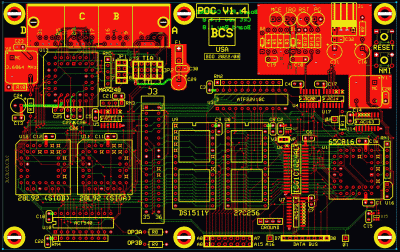
poc_v14_pcb.gif [ 408.57 KiB | Viewed 167315 times ]

V1.4’s bank $00 memory map is somewhat different than V1.3. Each I/O device occupies 128 bytes of address space, compared to the 256 bytes that older POC versions have used. Also, there is no mirroring in the I/O block. So instead of I/O extending from $00C000 to $00CFFF, as it did in V1.2 and V1.3, it now occupies $00C000 to $00C3FF. As a result, previously-inaccessible RAM from $00C400 to $00CFFF is now exposed, for a total of 3KB. That RAM will be “owned” by the system firmware, and will have enough room for direct page (256 bytes), the hardware stack (256 bytes), the serial I/O queues (2048 bytes), and BIOS kernel and M/L monitor workspace (512 bytes). Everything in bank $00 below $00C000 will be unencumbered, as will be the case with bank $01 RAM. ROM will continue to be visible from $00D000 to $00FFFF.

One of the benefits of the new memory map is applications can set the top-of-stack and start of direct page anywhere below $C000 without interfering with the firmware. That gives applications 48KB of contiguous bank $00 RAM for their direct pages and stacks. As firmware API calls are via software interrupts, applications can run equally well in bank $01, which makes possible having TSR programs loaded and readily available when needed (a feature also possible in POC V1.3, although with less bank $00 “elbow room”). This capability is made possible by the relative ease at which 65C816 programs can be made relocatable.

Hardware-wise, there’s the GAL, an ATF22V10C, to replace all of the discrete address-decoding logic used in the old POC versions. I was able to get hold of the somewhat-elusive 7.5ns part, so I’m not expecting any timing contretemps (famous last words :D). As the 22V10 has only 10 dedicated outputs, I am still dependent on some discrete logic, namely an OR gate to produce a valid address signal (VADR, which is VDA | VPA) for the GAL’s benefit. Since it is the only use of an OR gate in the circuit, I designed around a LVC1G part, which economizes PCB real estate consumption. Plus the LVC1G part is slightly faster than AC or AHC logic.

Clock generation is completely different than that of V1.3. V1.4 uses a synchronous counter (74AC163) to produce Ø2, which is an approach I tested in V1.2 (which was stable at 20 MHz), that having been derived from Jeff’s clock-stretching circuit. As a Ø1 clock (inverted Ø2) is needed to gate the bank bits latch, and the counter doesn’t have a complement to its QD output, a 74LVC1G04 inverter that is driven from QD does the honors. The inverter introduces approximately 3 to 4 ns prop time (a bit less than with 74AC or 74AHC logic), but as an experiment, I skipped the series resistor I usually have in clock circuits to suppress ringing. Ø2 continues to pass through series resistance, which introduces a small amount of lag in the signal (apparently 2-3 ns, from observations made on POC V1.3). The result is the two clocks should be very close to being 180 degrees out of phase. The logic analyzer will tell the tale when I get this thing built. If this works as I hope it will, I should be able to clock the system at 20 MHz.

Construction-wise, V1.4 will be built on the usual four-layer board. I’ve included a lot of test points to facilitate observation, include the entire address space, data bus and some other signals. I’m also using a slot for expansion, which is more reliable than the pin arrangement used in older POC versions. One other change I made was to mount the real-time clock on the main board in its own socket. Previously, the RTC had to be mounted on whatever was going to be plugged into expansion, which was inconvenient from a design standpoint. Reserving space on the PCB necessitated an increase in board size to get the clock to fit. The increase is negligible.

I’ve got parts on order and as soon as I get them, I’ll verify clearances on the PCB and then get it made.

_________________
x86?  We ain't got no x86.  We don't NEED no stinking x86!


Top
 Profile  
Reply with quote  
PostPosted: Wed Sep 07, 2022 2:03 am 
Offline
User avatar

Joined: Thu May 28, 2009 9:46 pm
Posts: 8178
Location: Midwestern USA
As I was preparing the bill of materials for POC V1.4 and getting ready to order, I started running into some issues with getting parts. A big one is the MAX248 TIA-232 transceiver, which has skyrocketed in price and is closing in on $40 each. The MAX248 is very convenient because all four TIA-232 channels can be interfaced through it in both directions—a one-chip solution. However, the cheap Irishman in me refuses to pay nearly $40 for something that was only $16 when I built POC V1.3.

I decided to modify the design to use two MAX238s, for a total cost of $14, including the charge pump and bypass capacitors (10 total). Only slightly more PCB space is needed. While I was at it, I decided to add a data bus transceiver, which I had omitted from the original design. Modified schematic and PCB layout attached.

Attachment:
File comment: POC V1.4 Schematic
pocv140.pdf [377.59 KiB]
Downloaded 48 times

Attachment:
File comment: POC V1.4 PCB
poc_v14_pcb.gif
poc_v14_pcb.gif [ 411.99 KiB | Viewed 167237 times ]

_________________
x86?  We ain't got no x86.  We don't NEED no stinking x86!


Top
 Profile  
Reply with quote  
PostPosted: Thu Sep 08, 2022 2:41 am 
Offline
User avatar

Joined: Tue Mar 05, 2013 4:31 am
Posts: 1373
Yes, some component prices have gotten out of hand. New PCB looks great... just wondering why you didn't use a single latch component (SN74LVC1G373) instead of the '573 octal latch, as only one of the 8 is being used. Just curious...

_________________
Regards, KM
https://github.com/floobydust


Top
 Profile  
Reply with quote  
PostPosted: Thu Sep 08, 2022 6:00 am 
Offline
User avatar

Joined: Thu May 28, 2009 9:46 pm
Posts: 8178
Location: Midwestern USA
floobydust wrote:
Yes, some component prices have gotten out of hand. New PCB looks great... just wondering why you didn't use a single latch component (SN74LVC1G373) instead of the '573 octal latch, as only one of the 8 is being used. Just curious...

The SOT-23 version of the 74LVC1G373 is currently unobtanium. Lead times for that part are stretching out to March of next year. I don’t want to go smaller than SOT-23 if possible.

The 74AC573 in SOIC is readily available in large quantities. Seven latches are being wasted, but so be it.

_________________
x86?  We ain't got no x86.  We don't NEED no stinking x86!


Top
 Profile  
Reply with quote  
PostPosted: Sat Sep 24, 2022 6:30 am 
Offline
User avatar

Joined: Thu May 28, 2009 9:46 pm
Posts: 8178
Location: Midwestern USA
As previously mentioned, most of the glue logic in POC V1.4 will be implemented in a GAL. Here is the CUPL code, which has a fatal defect:

Code:
/*
* * * * * * * * * * * * * * * * * * * * * * * * * * * * * * * * * * * * * * * * * *
*                                                                                 *
*                 W65C816S PROOF OF CONCEPT SINGLE-BOARD COMPUTER                 *
*                                                                                 *
* =============================================================================== *
*                                                                                 *
*        Copyright (c)2022 by BCS Technology Limited.  All rights reserved.       *
*                                                                                 *
* Permission is hereby granted to use, copy, modify and distribute this software, *
* provided this copyright notice remains unaltered in the source code and  proper *
* attribution is given.  Redistribution, in any form, must be at no charge to the *
* end user.  This code or any part  thereof, including any derivation, MAY NOT be *
* incorporated into any package intended for sale unless written permission to do *
* so has been granted by the copyright holder.                                    *
* ------------------------------------------------------------------------------- *
* THERE IS NO WARRANTY OF ANY KIND WITH THIS SOFTWARE.                            *
*                                                                                 *
* While it is believed that all code will perform as intended,  the user  assumes *
* all risk in connection with the incorporation of this software into any system. *
*                                                                                 *
* * * * * * * * * * * * * * * * * * * * * * * * * * * * * * * * * * * * * * * * * *

* * * * * * * * * *
* VERSION HISTORY *
* * * * * * * * * *

Ver    Rev Date    Revision
--------------------------------------------------------------------------------
1.0.0  2022/08/13  Original version.
--------------------------------------------------------------------------------

     Memory Map
====================
$000000-$00BFFF  RAM
$00C000-$00C3FF  I/O
$00C400-$00CFFF  RAM
$00D000-$00FFFF  ROM
$010000-$01FFFF  RAM
====================

       I/O Block Map
===========================
$00C000  DUART #1
$00C080  DUART #2
$00C100  vQUART IRQ status
$00C180  Real-time clock
$00C200  Expansion select A
$00C280  Expansion select B
$00C300  Expansion select C
===========================
*/

Name        pocv14;
PartNo      C220813001;
Date        2022/08/13;
Revision    1.0.0;
Designer    BDD;
Company     BCS Technology Limited;
Assembly    POC V1.4;
Location    U3;
Device      g22v10;

/*                          Signal            Type    Function                 */
/*=============================================================================*/
pin  1                    = A15;           /* input   address line             */
pin  2                    = A14;           /* input   address line             */
pin  3                    = A13;           /* input   address line             */
pin  4                    = A12;           /* input   address line             */
pin  5                    = A11;           /* input   address line             */
pin  6                    = A10;           /* input   address line             */
pin  7                    = A9;            /* input   address line             */
pin  8                    = A8;            /* input   address line             */
pin  9                    = A7;            /* input   address line             */
pin 10                    = A16;           /* input   address line             */
pin 11                    = VADDR;         /* input   valid address            */
pin 13                    = RWB;           /* input   read/write               */
pin 14                    = !WSE;          /* output  wait-state enable        */
pin 15                    = !RAM;          /* output  RAM select               */
pin 16                    = !ROM;          /* output  ROM select               */
pin 17                    = !RTC;          /* output  RTC select               */
pin 18                    = !XIOC;         /* output  expansion C select       */
pin 19                    = !XIOB;         /* output  expansion B select       */
pin 20                    = !XIOA;         /* output  expansion A select       */
pin 21                    = !SIOQ;         /* output  vQUART IRQ status select */
pin 22                    = !SIOB;         /* output  DUART #2 select          */
pin 23                    = !SIOA;         /* output  DUART #1 select          */
/*=============================================================================*/

field addr = [A15..A7];                    /* effective address LSW            */

/*
* * * * * * * * * *
* LOGIC EQUATIONS *
* * * * * * * * * *
*/

RAM  = VADDR & (addr:['h'00xx..BFxx] # addr:['h'C4xx..CFxx] # A16);

SIOA = VADDR & !A16 & addr:['h'C00x..C07x];

SIOB = VADDR & !A16 & addr:['h'C08x..C0Fx];

SIOQ = VADDR & !A16 & addr:['h'C10x..C17x];

RTC  = VADDR & !A16 & addr:['h'C18x..C1Fx];

XIOA = VADDR & !A16 & addr:['h'C20x..C27x];

XIOB = VADDR & !A16 & addr:['h'C28x..C2Fx];

XIOC = VADDR & !A16 & addr:['h'C30x..C37x];

ROM  = VADDR & !A16 & addr:['h'D0xx..FFxx] & RWB;

WSE  = VADDR & !A16 & (addr:['h'C0xx..C3Fx] # addr:['h'D0xx..FFxx]);

/*
   * * * * * * * * * * * * * * * * * * *
   * * * * * * * * * * * * * * * * * * *
   * * * * * * * * * * * * * * * * * * *
   * * *                           * * *
   * * *   E N D   O F   F I L E   * * *
   * * *                           * * *
   * * * * * * * * * * * * * * * * * * *
   * * * * * * * * * * * * * * * * * * *
   * * * * * * * * * * * * * * * * * * *
*/

The above code looks correct and in fact, the logic statements are all correct. However, any attempt to compile it crashes WinCUPL.

Next, here’s code that will compile and simulate:

Code:
/*
* * * * * * * * * * * * * * * * * * * * * * * * * * * * * * * * * * * * * * * * * *
*                                                                                 *
*                 W65C816S PROOF OF CONCEPT SINGLE-BOARD COMPUTER                 *
*                                                                                 *
* =============================================================================== *
*                                                                                 *
*        Copyright (c)2022 by BCS Technology Limited.  All rights reserved.       *
*                                                                                 *
* Permission is hereby granted to use, copy, modify and distribute this software, *
* provided this copyright notice remains unaltered in the source code and  proper *
* attribution is given.  Redistribution, in any form, must be at no charge to the *
* end user.  This code or any part  thereof, including any derivation, MAY NOT be *
* incorporated into any package intended for sale unless written permission to do *
* so has been granted by the copyright holder.                                    *
* ------------------------------------------------------------------------------- *
* THERE IS NO WARRANTY OF ANY KIND WITH THIS SOFTWARE.                            *
*                                                                                 *
* While it is believed that all code will perform as intended,  the user  assumes *
* all risk in connection with the incorporation of this software into any system. *
*                                                                                 *
* * * * * * * * * * * * * * * * * * * * * * * * * * * * * * * * * * * * * * * * * *

* * * * * * * * * *
* VERSION HISTORY *
* * * * * * * * * *

Ver    Rev Date    Revision
--------------------------------------------------------------------------------
1.0.0  2022/08/13  Original version.
--------------------------------------------------------------------------------

    Memory Map
==================
000000-00BFFF  RAM
00C000-00C3FF  I/O
00C400-00CFFF  RAM
00D000-00FFFF  ROM
010000-01FFFF  RAM
==================

       I/O Block Map
==========================
00C000  DUART #1
00C080  DUART #2
00C100  vQUART IRQ status
00C180  Real-time clock
00C200  Expansion select A
00C280  Expansion select B
00C300  Expansion select C
==========================
*/

Name        pocv14;
PartNo      C220813001;
Date        2022/08/13;
Revision    1.0.0;
Designer    BDD;
Company     BCS Technology Limited;
Assembly    POC V1.4;
Location    U3;
Device      g22v10;

/*=============================================================================*/
pin  1                    = A15;           /* input   address line             */
pin  2                    = A14;           /* input   address line             */
pin  3                    = A13;           /* input   address line             */
pin  4                    = A12;           /* input   address line             */
pin  5                    = A11;           /* input   address line             */
pin  6                    = A10;           /* input   address line             */
pin  7                    = A9;            /* input   address line             */
pin  8                    = A8;            /* input   address line             */
pin  9                    = A7;            /* input   address line             */
pin 10                    = A16;           /* input   address line             */
pin 11                    = VADDR;         /* input   valid address            */
pin 13                    = RWB;           /* input   read/write               */
pin 14                    = !WSE;          /* output  wait-state enable        */
pin 15                    = !RAM;          /* output  RAM select               */
pin 16                    = !ROM;          /* output  ROM select               */
pin 17                    = !RTC;          /* output  RTC select               */
pin 18                    = !XIOC;         /* output  expansion C select       */
pin 19                    = !XIOB;         /* output  expansion B select       */
pin 20                    = !XIOA;         /* output  expansion A select       */
pin 21                    = !SIOQ;         /* output  vQUART IRQ status select */
pin 22                    = !SIOB;         /* output  DUART #2 select          */
pin 23                    = !SIOA;         /* output  DUART #1 select          */
/*=============================================================================*/

field addr = [A15..A7];                    /* effective address LSW            */

/*
* * * * * * * * * *
* LOGIC EQUATIONS *
* * * * * * * * * *
*/

RAM  = VADDR & (addr:['h'00xx..BFxx] # addr:['h'C4xx..CFxx] # A16);

SIOA = VADDR & !A16 & addr:['h'C00x..C07x];

SIOB = VADDR & !A16 & addr:['h'C08x..C0Fx];

SIOQ = VADDR & !A16 & addr:['h'C10x..C17x];

RTC  = VADDR & !A16 & addr:['h'C18x..C1Fx];

XIOA = VADDR & !A16 & addr:['h'C20x..C27x];

XIOB = VADDR & !A16 & addr:['h'C28x..C2Fx];

XIOC = VADDR & !A16 & addr:['h'C30x..C37x];

ROM  = VADDR & !A16 & addr:['h'D0xx..FFxx] & RWB;

WSE  = VADDR & !A16 & (addr:['h'C0xx..C3Fx] # addr:['h'D0xx..FFxx]);

/*
   * * * * * * * * * * * * * * * * * * *
   * * * * * * * * * * * * * * * * * * *
   * * * * * * * * * * * * * * * * * * *
   * * *                           * * *
   * * *   E N D   O F   F I L E   * * *
   * * *                           * * *
   * * * * * * * * * * * * * * * * * * *
   * * * * * * * * * * * * * * * * * * *
   * * * * * * * * * * * * * * * * * * *
*/

Can anyone spot the difference between the two renditions? :D

_________________
x86?  We ain't got no x86.  We don't NEED no stinking x86!


Top
 Profile  
Reply with quote  
PostPosted: Sat Sep 24, 2022 1:17 pm 
Offline
User avatar

Joined: Tue Mar 05, 2013 4:31 am
Posts: 1373
Well, a quiz first thing in the morning.... I don't do well with morning exams, but....

Looks like the pesky "$" signs in front of the commented section of Memory and I/O Block maps hosed up WinCUPL... but there is the extra commented part further down in the second file, but that wouldn't/shouldn't cause anything.

Passing grade??

_________________
Regards, KM
https://github.com/floobydust


Top
 Profile  
Reply with quote  
PostPosted: Sat Sep 24, 2022 2:35 pm 
Offline
User avatar

Joined: Wed Jul 27, 2022 6:14 am
Posts: 54
i just processed your files with cupl itsself and it says:

Code:
c:\Wincupl\Shared\cupl.exe -xu c:\wincupl\shared\atmel.dl  2
cuplx
[0010cx] line(35) invalid preprocessor command:  $000000-$00bfff
[0010cx] line(36) invalid preprocessor command:  $00c000-$00c3ff
[0010cx] line(37) invalid preprocessor command:  $00c400-$00cfff
[0010cx] line(38) invalid preprocessor command:  $00d000-$00ffff
[0010cx] line(39) invalid preprocessor command:  $010000-$01ffff
[0010cx] line(44) invalid preprocessor command:  $00c000
[0010cx] line(45) invalid preprocessor command:  $00c080
[0010cx] line(46) invalid preprocessor command:  $00c100
[0010cx] line(47) invalid preprocessor command:  $00c180
[0010cx] line(48) invalid preprocessor command:  $00c200
[0010cx] line(49) invalid preprocessor command:  $00c280
[0010cx] line(50) invalid preprocessor command:  $00c300


so $ in the first col means a preprocessor command for cupl. Even if it's in a comment, the preprocessor doesn't care about commands. To solve simply put a space before the $ sign...

_________________
don't count on me, i'm engineer (Animotion)
my arduino pages: http://rcarduino.de


Top
 Profile  
Reply with quote  
Display posts from previous:  Sort by  
Post new topic Reply to topic  [ 564 posts ]  Go to page Previous  1 ... 32, 33, 34, 35, 36, 37, 38  Next

All times are UTC


Who is online

Users browsing this forum: No registered users and 6 guests


You cannot post new topics in this forum
You cannot reply to topics in this forum
You cannot edit your posts in this forum
You cannot delete your posts in this forum
You cannot post attachments in this forum

Search for:
Jump to: