6502.org Forum  Projects  Code  Documents  Tools  Forum
It is currently Sun May 05, 2024 6:11 am

All times are UTC


Post new topic Reply to topic  [ 564 posts ]  Go to page Previous  1 ... 18, 19, 20, 21, 22, 23, 24 ... 38  Next
Author Message
 Post subject: Re: POC Computer
PostPosted: Wed Apr 29, 2015 3:28 pm 
Offline
User avatar

Joined: Thu May 28, 2009 9:46 pm
Posts: 8173
Location: Midwestern USA
floobydust wrote:
Regardless, neither chip will give you a jiffy clock that is 100Hz...For my 65C02 system, I used the 65C22 timer as a free-running counter but does require that you set the timer value based on the CPU clock rate. I'm using a 4ms (250Hz) value which can be accurately configured for typical CPU clock rates from 1- to 16MHz. Of course the can oscillator precision varies a bit from unit to unit as I have 3 systems running concurrently and they all drift a bit differently.

I currently have POC running with the DUART generating the jiffy IRQ, and having it report the date and time, along with uptime, at one hour intervals. So far the uptime is accurately tracking the time of day.

_________________
x86?  We ain't got no x86.  We don't NEED no stinking x86!


Top
 Profile  
Reply with quote  
 Post subject: Re: POC Computer
PostPosted: Wed Apr 29, 2015 3:31 pm 
Offline
User avatar

Joined: Thu Dec 11, 2008 1:28 pm
Posts: 10797
Location: England
Although it seems unlikely to be an explanation, it's true that 324 is about 1% shy of 327.68, and 324 is 4 * 9 * 9, so a cascade of simple dividers can provide the approx 10ms clock at low power - slightly lower power, perhaps, than a 9-bit counter and comparator.


Top
 Profile  
Reply with quote  
 Post subject: Re: POC Computer
PostPosted: Wed Apr 29, 2015 3:32 pm 
Offline
User avatar

Joined: Thu May 28, 2009 9:46 pm
Posts: 8173
Location: Midwestern USA
BigEd wrote:
Interesting... I can't presently see how it manages to be 1% fast. The 10ms granularity of setting the watchdog period would mean the counter needs to tick every 327.68 ticks - if it ticks every 327 ticks then it would be 0.2% fast.

It would be interesting to know what accuracy you'd see if you ran with a 20ms watchdog instead of 10ms.

The one percent number is approximate and is based upon observing how long a time delay actually took to expire.

I suspect that as the period increases the cumulative inaccuracy would decrease, only becoming zero if the watchdog period is an exact sub-multiple of the time base period. I could probably prove that by running the watch dog at one second per IRQ and reworking the interrupt service routine to skip the jiffy count update and directly increment the clock values.

_________________
x86?  We ain't got no x86.  We don't NEED no stinking x86!


Top
 Profile  
Reply with quote  
 Post subject: Re: POC Computer
PostPosted: Sat Mar 18, 2017 5:37 am 
Offline
User avatar

Joined: Thu May 28, 2009 9:46 pm
Posts: 8173
Location: Midwestern USA
It's been nearly two years since I last posted anything in this topic. Since then, I made some detail changes to the firmware, but other than that, development on POC V1 has come to an end and I have moved on to POC V2. A final note, however.

POC V1.1 is stable at 12.5 MHz with the SCSI host adapter plugged in. At that speed, compute-bound performance is excellent. SCSI performance is approximately 720KB/second with a 32KB (64 block) read or write to a hard disk. This is very close to the theoretical limit of 745KB/second, and not at all bad for what is essentially programmed I/O operation.

The unit will boot at 15 MHz sans the SCSI host adapter, using a 45ns ROM (Atmel 27C256 OTP). This is 1 MHz beyond the official 14 MHz rating of the 65C816. POC V1.1 uses only discrete 74AC logic (all PDIP parts) and an NXP 28L92 DUART, whose bus timing specs are fast enough to operate at 15 MHz without wait-stating. However, at this speed, the cycle time is 66.7ns, so it's clear I'm crowding the ROM's timing specs.

I believe 15 MHz operation is possible because I do not qualify chip selects with Ø2, which gives RAM, ROM and I/O a maximum amount of time to get ready for access. It also helps that the operating environment is voltage- and temperature-friendly. I suspect if the environment got warmer, the power supply's 5 volt output sagged, or both happened, the machine might falter.

What this project did prove is that high speed operation of the 65Cxx family is possible with discrete logic, as long as close attention is paid to proper device qualification, board layout, clock quality and choice of components. My original goal was to achieve stable operation at 8 MHz. I think I met that goal with room to spare. :)

_________________
x86?  We ain't got no x86.  We don't NEED no stinking x86!


Top
 Profile  
Reply with quote  
PostPosted: Thu Dec 19, 2019 12:19 am 
Offline
User avatar

Joined: Thu May 28, 2009 9:46 pm
Posts: 8173
Location: Midwestern USA
POC V1.2

This is a bump to a dormant topic that has seen quite a bit of activity. Based upon that, I figured someone might be interested in more of the twists and turns my computer-building activities have taken.

In another topic, I posted:

Quote:
I think I leaped too far ahead with POC V2. The combination of programmable logic and the four serial I/O channels running in a QUART that was unfamiliar to me proved to be too much to debug all at one time, especially given the test gear at my disposal. My new something will be a discrete logic unit (74AC) with four serial channels using two 28L92 DUARTs. The logic will be more-or-less modeled on POC V1.1, which is (apparently) bug-free and rock-solid at 12.5 MHz. I'll be posting more about this once I have a design worked out and a schematic drawn.

I've completed a preliminary design for a unit I've dubbed POC V1.2. Here's the schematic:

Attachment:
File comment: POC V1.2 Schematic
poc12.pdf [340.73 KiB]
Downloaded 135 times

Salient features are:

  • 65C816 MPU, running at clock speeds up to 14 MHz (I hope!).
  • Four high-speed TIA-232 serial channels using a "virtual QUART" (vQUART).
  • Console configurable for TIA-232 or TTL operation.
  • 512KB of static RAM, 48KB in "base RAM" and 448KB of "extended RAM" (there's a typo in the schematic that says 484KB).
  • 12KB of ROM.
  • 4KB I/O space, although only 2KB is actually decoded.
  • 74AC and 74ACT logic.

Cascaded discrete logic scales up propagation time and hence sets a hard limit on how fast the unit will reliably run. In POC V1.0 and V1.1, a design goal was to put no more than two gates between a chip select and the address bus. This goal cannot be entirely met in V1.2 due to logic needed to handle A16-A18 generation. Also, some complication was added to prevent ROM and I/O from being mirrored in banks other than bank $00—the result will be contiguous RAM from $010000 to $07FFFF.

Despite the more elaborate glue logic, a timing analysis suggests that performance should be close to what was achieved in V1.1, as much the logic I am using can achieve single digit prop times. Rearranging the memory map so I/O and ROM are contiguous helped to keep a lid on how much cascaded logic will be required.

You may be wondering why I am regressing in this fashion. The POC V2 designs have stubbornly resisted debugging attempts, and the added complication of four serial channels is part of it. My purpose with this design is to eliminate uncertainties that may exist with programmable logic so I can successfully develop a trustworthy vQUART driver. Once that has been accomplished I should be able to go back to POC V2 knowing serial I/O will work. That should substantially reduce debugging difficulty—so I think.

As for actually building the contraption, I face a conundrum. Just about all of the devices needed are still available in DIP packages, which I am still able to handle despite loss of vision in one eye. However, a DIP design will result in a large PCB and lead to possible issues due to the effects of long traces. So I may end up deciding that I can't build it after I've worked out a board layout.

_________________
x86?  We ain't got no x86.  We don't NEED no stinking x86!


Last edited by BigDumbDinosaur on Sun Jan 19, 2020 7:38 am, edited 1 time in total.

Top
 Profile  
Reply with quote  
PostPosted: Thu Dec 19, 2019 4:28 pm 
Offline
User avatar

Joined: Wed Feb 14, 2018 2:33 pm
Posts: 1403
Location: Scotland
BigDumbDinosaur wrote:
As for actually building the contraption, I face a conundrum. Just about all of the devices needed are still available in DIP packages, which I am still able to handle despite loss of vision in one eye. However, a DIP design will result in a large PCB and lead to possible issues due to the effects of long traces. So I may end up deciding that I can't build it after I've worked out a board layout.


I'd suggest that you do it anyway. Get it as good as you can within time/finances and see what happens. That was mostly my approach and I was very pleasantly surprised when I got it to 16Mhz. The 8-bit guy's runs at 8Mhz for the most part and that's a fairly big PCB.

Good luck - looks very interesting. Those UARTs.. Hmm.. And space (if I understand it rightly), for 3 additional devices. I think, personally, I'd swap out one of the DUART chips for a 65C22. Do you think you'll use all 4 uarts?


-Gordon

_________________
--
Gordon Henderson.
See my Ruby 6502 and 65816 SBC projects here: https://projects.drogon.net/ruby/


Top
 Profile  
Reply with quote  
PostPosted: Thu Dec 19, 2019 6:23 pm 
Offline
User avatar

Joined: Thu May 28, 2009 9:46 pm
Posts: 8173
Location: Midwestern USA
drogon wrote:
I'd suggest that you do it anyway. Get it as good as you can within time/finances and see what happens.

Cost per se is not much of a concern, as long as I don't end up with a PCB the size of an EATX server motherboard. It'll come down to whether I feel I can build it. The DIP stuff would be easy, but will use up a lot of space and make for messy routing of some circuits. The SRAM is an SOJ-36 part, which is unavoidable. Soldering one is out of the question for me unless I decide to splurge, get a stencil made and reflow the board (I have the requisite oven to do so). If I am going to do that I might as well go SMT all the way. However, I will be struggling to correctly place the parts due to that pesky vision problem.

Quote:
Those UARTs.. Hmm.. And space (if I understand it rightly), for 3 additional devices. I think, personally, I'd swap out one of the DUART chips for a 65C22. Do you think you'll use all 4 uarts?

Eliminating one DUART and substituting a 65C22 won't save much space (although it would eliminate one MAX238). In any case, the 65C22 doesn't offer anything that I need, plus it is annoyingly slaved to Ø2.

I have three terminals (actually thin clients with serial I/O) at my disposal, plus high-speed serial I/O on my development server. One of V1.2's serial ports will be used for the console terminal and the second one for data transfers between the development server and V1.2. I have plans to work on a preemptive, multitasking kernel, the testing of which would be expedited by having two terminals running independently of the console. So, yes, I will use all four serial channels.

_________________
x86?  We ain't got no x86.  We don't NEED no stinking x86!


Top
 Profile  
Reply with quote  
PostPosted: Thu Dec 26, 2019 2:54 am 
Offline
User avatar

Joined: Thu May 28, 2009 9:46 pm
Posts: 8173
Location: Midwestern USA
BigDumbDinosaur wrote:
I've completed a preliminary design for a unit I've dubbed POC V1.2...As for actually building the contraption, I face a conundrum...a DIP design will result in a large PCB...

A design using DIP packages worked out to 30 square inches (76.2 sq cm), and that with everything tightly jammed together, not particularly good for trace routing. A design with SOIC packages works out to 24 square inches (61 sq cm) and that's with more comfortable parts spacing. If this thing is going to get built it will have to be with the SOIC stuff.

Attachment:
File comment: POC V1.2 PCB
poc1.2pcb.gif
poc1.2pcb.gif [ 101.58 KiB | Viewed 9358 times ]

BTW, some of that seemingly wasted space on the above board may eventually get used. I made the board perimeter somewhat larger than needed.

_________________
x86?  We ain't got no x86.  We don't NEED no stinking x86!


Top
 Profile  
Reply with quote  
PostPosted: Sat Jan 04, 2020 12:48 am 
Offline
User avatar

Joined: Thu May 28, 2009 9:46 pm
Posts: 8173
Location: Midwestern USA
BigDumbDinosaur wrote:
I've completed a preliminary design for a unit I've dubbed POC V1.2...

Upon sleeping on this a bit, I re-evaluated my goals and decided to simplify the design. I removed the extended addressing function, as it isn't germane to BIOS development.

The main purpose of building V1.2 is to create a machine on which I can concoct a virtual QUART (vQUART, vQUART meaning "virtual quad UART") driver, as well as a BIOS API that is called with software interrupts instead of subroutine calls. As long as I have a reasonable amount of ROM and bank zero RAM available it will all work without the complication of extended addressing. Eliminating extended addressing means less glue logic will be required, which means fewer gates and hence more timing headroom. It also means I can use a smaller SRAM. Fewer gates means fewer chips on the board, which, as you will see, will allow me to use "vision-friendly" DIP packages for all logic devices (alas, the SRAM is only available in SMT, and space constraints require that I use the SOIC version of the MAX238 transceiver). Below is the schematic and PCB for this unit:

Attachment:
File comment: POC V1.2.1 Schematic
poc12.pdf [306.33 KiB]
Downloaded 76 times
Attachment:
File comment: POC V1.2.1 PCB Layout
poc_v1.2_pcb.gif
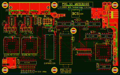
poc_v1.2_pcb.gif [ 97.58 KiB | Viewed 9288 times ]

The vQUART consists of two NXP 28L92 DUARTs whose driver will make them appear to be a single QUART to applications that access serial I/O (SIO) through the BIOS. Of the four SIO channels, channel A will be the console channel, channel B will be a hardwired link to my Linux software development machine, and channels C and D will be uncommitted. A BIOS call for SIO services will use the .X register as the zero-based channel index, which is convenient for higher-level applications. As is the case for my DUART drivers, everything will be interrupt-driven and will take full advantage of the 28L92's 16-deep FIFOs.

Speaking of interrupts, the 28L92 can be configured so general purpose output pins 4, 5, 6 and 7 (OP4-7) act as open-drain IRQ signals. OP4 is wired to the RxD channel 1 IRQ, OP5 is wired to the RxD channel 2 IRQ, and OPs 6 and 7 are wired to the channel 1 and channel 2 transmitters, respectively. When the 28L92 interrupts with its main IRQ output, it will also pull one or more of these pins low if reception and/or transmission activity was the cause of the interrupt.

In order to take advantage of this feature, I have the OPs wired to the inputs of a 74ACT540 bus driver, with bits 0-3 wired to the receiver IRQs and bits 4-7 wired to transmitter IRQs—bits 0 and 4 are channel A, bits 1 and 5 are channel B, and so forth. The bus driver is assigned a location in the I/O map (designated SIOQ) which when read, will return a real-time IRQ status. If %00000000 is read, then no receive or transmit IRQs were generated. Otherwise, bits will be set according to what interrupted. These bits are real-time, meaning they stay set until the cause of the IRQ has been cleared.

This arrangement doesn't report the cause of other vQUART IRQs, such as timer underflow, which must be detected by reading the individual DUART interrupt status registers. However, the interrupt service handler's work will greatly reduced, since no polling of each receiver and transmitter will be required. This reduction becomes important when one considers that if all four channels are simultaneously receiving and transmitting at 115.2Kbps, as many as 46,080 IRQs due to SIO activity could occur in one second, assuming an IRQ occurs with each datum received or sent. In practice, the rate won't be quite as severe, due to the buffering provided by the DUARTs' FIFOs. In the best case, 2880 IRQs would occur each second of continuous bi-directional communication, as an interrupt will only come when a receiver FIFO is full or a transmitter FIFO is empty.

Having two 28L92s in the circuit means I will have two precision timers (timers A and B) available, with timer A generating a 100 Hz jiffy IRQ for timekeeping purposes. I've yet to come up with a use for the other timer, but I'm sure I'll think of something. A useful feature of the 28L92 is the timer's output can be directed to the OP3 pin to drive something external—a pullup resistor is required to use this feature. In timer mode, a continuous square wave equal to the timer's underflow rate is produced, where as in counter mode, OP3 is high until the timer underflows, at which time it goes low.

As well as developing the vQUART driver, I will be implementing an interrupt-driven BIOS API. Instead of calling a BIOS API function with JSR, the COP instruction, along with an API function value (API index), will be used to cause a software interrupt, which will be intercepted by the BIOS. There a couple of ways this can be implemented:

  1. Use COP's signature byte as an index. This method is analogous to the method used in PC hardware to call BIOS services. It has the advantage of not using any of the registers, leaving them free for passing parameters. It has the disadvantage of requiring convoluted bank-twiddling operations in the BIOS' API front-end code to fetch the index, producing relatively slow performance.

  2. Push the index to the stack. This method also has the advantage of leaving the registers available for parameter passing. Compared to method 1 above, this method has the disadvantage of requiring that the caller push the index, which is an extra step in calling the API, as well as API front end activity to fetch the index and rebalance the stack.

  3. Pass the index in a register. This method has the advantage of having the least effect on performance, as no stackrobatics or bank twiddling is required to pass and fetch the API index. It has the disadvantage of using a register, which means parameter passing is made more complicated.

In POC V1.1's BIOS, only the registers are used for parameter passing, as no function requires more than three parameters. Obviously, if more than three parameters must be passed there is going to be a problem. Which of the above methods to use is something I will be kicking around as things progress.

In any case, the value of using a software interrupt to call API services is it is bank-agnostic. In a system with more than 64KB, a program can call the BIOS API—which must be in bank zero—without having to do anything special to compensate for not being in bank zero. This will be a very useful feature when I finally get a machine with more than 64KB running.

_________________
x86?  We ain't got no x86.  We don't NEED no stinking x86!


Top
 Profile  
Reply with quote  
PostPosted: Tue Jan 07, 2020 8:49 pm 
Offline
User avatar

Joined: Wed Aug 17, 2005 12:07 am
Posts: 1207
Location: Soddy-Daisy, TN USA
BDD,

I can't remember if I've offered before, but I would be more than happy to solder up a board for you. Even SMD parts. Free of charge.

Anyway, just an offer.

Either way...I really look forward to seeing more of this design!

_________________
Cat; the other white meat.


Top
 Profile  
Reply with quote  
PostPosted: Tue Jan 07, 2020 10:01 pm 
Offline
User avatar

Joined: Thu May 28, 2009 9:46 pm
Posts: 8173
Location: Midwestern USA
cbmeeks wrote:
BDD,

I can't remember if I've offered before, but I would be more than happy to solder up a board for you. Even SMD parts. Free of charge.

Anyway, just an offer.

Either way...I really look forward to seeing more of this design!

Thanks for your offer. I will have help to solder the three SMDs on my revised layout. The DIP stuff I can do, thanks to a recently-acquired vision aid.

The next iteration of POC V1 will be the design with extended RAM. That will be all SMT, as doing it in DIP results in an excessively large PCB, as well as layout headaches. I will likely take you up on your offer when that version comes off the drawing board.

BTW, here is the current board layout.

Attachment:
File comment: POC V1.2 Printed Circuit Board
poc_v1.2_pcb.gif
poc_v1.2_pcb.gif [ 101.31 KiB | Viewed 9226 times ]

By pushing around the board perimeters here and there, I was able to use DIP for all of the glue logic—only the SRAM and the two MAX238s are SMT. I even found enough room to rig up a "heartbeat" indicator (bottom of PCB in between center and right-hand mounting holes). :D The heartbeat circuit is hooked up to the MPU's /IRQ input, so when there is IRQ activity the LED will flash. This feature should be useful in debugging the vQUART driver. If the LED stops flashing then the interrupt system has gone belly-up.

During the revised layout exercise, it became evident that mounting the SRAM north-south would be more space-efficient than east-west. As it turned out, doing so slightly reduced the number of via required, meaning fewer holes and hence some cost reduction in the board (not much, but every bit helps). This SRAM layout is very similar to what I used in POC V1.1.

As part of this project, I've developed a new board layout for anything that plugs into the expansion port. My original layout was an "after the fact" concoction meant to add SCSI to POC V1.0 by using the real-time clock socket as the expansion port. Accordingly, I had to work within the layout constraints of that design. Since I had to reshape the PCB to accommodate the V1.2 circuit design, I decided it was time to come up with a more sane expansion board layout. My first use for it will be a new SCSI host adapter design with active termination and support for higher bus speeds.

Farther down the road before I put POC V1.x back into the closet is to develop a version that uses a real QUART, instead of the vQUART in this design. In the vQUART arrangement, the registers of the two DUARTs are not contiguous in the I/O memory map, which adds some complication to the driver code. The QUART's 32 registers will be contiguous, which aside from simplifying the driver, will free up an I/O select. The QUART has an interesting interrupt arbitration feature that I'd like to try to get working, plus it has additional outputs that can be used to report almost all IRQ sources in hardware.

First step is to get V1.2 upright with a pulse. That should happen soon.

_________________
x86?  We ain't got no x86.  We don't NEED no stinking x86!


Top
 Profile  
Reply with quote  
PostPosted: Wed Jan 08, 2020 5:52 am 
Offline
User avatar

Joined: Thu May 28, 2009 9:46 pm
Posts: 8173
Location: Midwestern USA
Something I had started doing a while ago was generating color-coded drawings of the logic circuits of my projects in an effort to catch design errors. So I did with POC V1.2.

V1.2's memory map is different than V1.0's and V1.1's. In the latter machines, RAM runs from $0000 to $CFFF (52KB), I/O from $D000-$DFFF (4KB) and ROM from $E000-$FFFF (8KB)—this is a "classic" 6502 memory map. As I added to the firmware in POC V1.1 it became clear that I was severely crowding that 8KB of ROM—the end of the firmware is at $FF50, which is only 144 bytes away from the start of the 65C816's hardware vectors at $FFE0.

The 27C256 ROM I use is a 32KB device, which means I have an unused 24KB. Mapping in another 4KB of ROM would give me the headroom I need for my planned firmware additions. With no need to maintain backward compatibility with V1.0 and V1.1, I decided to revamp the memory map, which is now RAM from $0000 to $BFFF (48KB), I/O from $C000 to $CFFF(4KB) and ROM from $D000 to $FFFF (12KB). Further to this, ROM will only appear on a read cycle—a write to the ROM's address range will go into the bit bucket.

After going through several iterations of glue logic, I came up with a circuit that meets my (unofficial) dictum that no more than two gates should be between the address bus and chip selects. With 74AC logic, this works out to an average of 14ns delay from address generation to chip select, more than enough timing headroom to support 14 MHz operation (although that technically isn't possible with the 55ns EPROM I am using). In order to prove on paper that the glue logic would work as required, I color-coded four possible machine states: RAM select with write¹, I/O select with write, ROM select with read and ROM select with write.

Attachment:
File comment: RAM Select at $BFxx, Write Cycle
ram_select_bfxx_write.gif
ram_select_bfxx_write.gif [ 396.81 KiB | Viewed 9210 times ]
Attachment:
File comment: I/O Select at $C000, Write Cycle
i_o_select_write.gif
i_o_select_write.gif [ 398.19 KiB | Viewed 9210 times ]
Attachment:
File comment: ROM Select at $D0xx, Write Cycle
rom_select_d000_write.gif
rom_select_d000_write.gif [ 398.24 KiB | Viewed 9210 times ]
Attachment:
File comment: ROM Select at $D0xx, Read Cycle
rom_select_d000_read.gif
rom_select_d000_read.gif [ 649.48 KiB | Viewed 9210 times ]

In the above illustrations, the net symbol VADR is the logical OR of the 65C816's VDA and VPA outputs, which means VADR goes high when the '816 is generating a valid address. All chip selects are qualified by this signal to avoid confusing devices with temporarily bogus addresses generated as the '816 sets up for the next operation.

The above glue logic is adaptable to the 65C02 with two changes: replacement of the 74ACT11030 AND gate with a 74AC20 and removal of the VADR logic, which has no analog in the 65C02. Note that the SRAM must be at least 48KB.
————————————————————————————————————————————————————————
¹I belatedly noticed that I mixed up the color-coding for A14 and A15 in the RAM select illustration. So the actual address would be $7Fxx, not $BFxx. Either way, the logic does work on paper.

_________________
x86?  We ain't got no x86.  We don't NEED no stinking x86!


Last edited by BigDumbDinosaur on Wed Jan 08, 2020 7:09 pm, edited 1 time in total.

Top
 Profile  
Reply with quote  
 Post subject: POC Computer Version One
PostPosted: Wed Jan 08, 2020 11:07 am 
Offline

Joined: Thu Apr 19, 2018 12:53 pm
Posts: 25
Hello BD,

Logic looks sound.
For Rom, why not use a 29F010 with 45nS access?
As far as I know, they're still available from Atmel. (And I have a couple in my stock)
The flash will also save some hassle programming Eproms. Of course the processor can reprogram the Flash. (Firmware available, written for MegaSpeedy and 65C02)
The excess memory could be mapped outside the first 64K or in a banking scheme, or just jumpers...

For ease of use, I put the QFP package on a PCB to make it DIL again. (I have a lot of those adapter PCB's as well)


Top
 Profile  
Reply with quote  
PostPosted: Wed Jan 08, 2020 7:04 pm 
Offline
User avatar

Joined: Thu May 28, 2009 9:46 pm
Posts: 8173
Location: Midwestern USA
Guus Assmann wrote:
For Rom, why not use a 29F010 with 45nS access?

I'm using the 27C256 for the same reason I'm using discrete logic: I know the combination works. The only hardware that is of concern is the vQUART setup. Using flash ROM will add uncertainty that will be a distraction from the purpose of this design, which is firmware development. In any case, I've got lots of AMD 27C256-55 EPROMs laying around, and they are DIP, not SMT. I know they are good for at least 12.5 MHz, plus I can easily program them and erase them en masse.

_________________
x86?  We ain't got no x86.  We don't NEED no stinking x86!


Top
 Profile  
Reply with quote  
PostPosted: Wed Jan 08, 2020 7:19 pm 
Offline
User avatar

Joined: Wed Aug 17, 2005 12:07 am
Posts: 1207
Location: Soddy-Daisy, TN USA
BigDumbDinosaur wrote:
In any case, I've got lots of AMD 27C256-55 EPROMs laying around


Maybe you could sell a few of them and buy yourself a new car, house, etc. Those things have gotten ridiculously expensive in recent years.

_________________
Cat; the other white meat.


Top
 Profile  
Reply with quote  
Display posts from previous:  Sort by  
Post new topic Reply to topic  [ 564 posts ]  Go to page Previous  1 ... 18, 19, 20, 21, 22, 23, 24 ... 38  Next

All times are UTC


Who is online

Users browsing this forum: No registered users and 13 guests


You cannot post new topics in this forum
You cannot reply to topics in this forum
You cannot edit your posts in this forum
You cannot delete your posts in this forum
You cannot post attachments in this forum

Search for:
Jump to: