6502.org Forum  Projects  Code  Documents  Tools  Forum
It is currently Tue Jun 25, 2024 5:27 am

All times are UTC


Post new topic Reply to topic  [ 45 posts ]  Go to page Previous  1, 2, 3  Next
Author Message
PostPosted: Fri Mar 17, 2023 8:42 am 
Offline
User avatar

Joined: Fri Nov 09, 2012 5:54 pm
Posts: 1397
5b) DSR# //input, no pullup

Wikipedia: DSR: DCE (modem) is ready to receive and send data.

MOS 6551 datasheet: (Data Set Ready)
"The low_active DSR# input pin is used to indicate to the 6551 the status of the modem.
A LOW indicated the "ready" state, and a HIGH "not-ready."

A transparent (half_static) latch samples the low_active signal from the DSR# input pad (the DSR# input latch),
and gives out DSR1#, which goes into "7a) Status register, Bit 6".

DCD1# also goes into an edge detector, which basically is built from a transparent (half_static) latch and an XOR gate.
The ede detector latch is loaded with DCD1# during a status register read (or when RX and TX are disabled with CMD0=0),
An XOR gate compares input and output of the edge detector latch,
and turns high_active signal DSR_CHANGED to HIGH if they are different.

DSR_CHANGED then freezes the DSR# input latch.
Because the DSR# input latch is frozen, DSR_CHANGED stays HIGH until the edge detector latch becomes transparent again
(or until a hardware reset).

DSR_CHANGED goes into "7a) Status register, Bit 7", which generates IRQ.

Attachment:
si8551r2_5b_dsr.png
si8551r2_5b_dsr.png [ 19.15 KiB | Viewed 435 times ]

Attachment:
8551r2_5b_dsr.png
8551r2_5b_dsr.png [ 53.3 KiB | Viewed 435 times ]


Top
 Profile  
Reply with quote  
PostPosted: Fri Mar 17, 2023 8:44 am 
Offline
User avatar

Joined: Fri Nov 09, 2012 5:54 pm
Posts: 1397
5c) DCD# //input, no pullup

Wikipedia: DCD: DCE (modem) is receiving a carrier from a remote DCE (another modem).

MOS 6551 datasheet: (Data Carrier Detect)
"The low_active DCD# input pin is used to indicate to the 6551 the status of the carrier-detect output of the modem.
A LOW indicates that the modem carrier signal is present, and a HIGH that it is not."

A transparent (half_static) latch samples the low_active signal from the DCD# input pad (the DCD# input latch),
and gives out DCD1#, which goes into "7a) Status register, Bit 5".

DCD1# also goes into an edge detector, which basically is built from a transparent (half_static) latch and an XOR gate.
The ede detector latch is loaded with DCD1# during a status register read (or when RX and TX are disabled with CMD0=0),
An XOR gate compares input and output of the edge detector latch,
and turns high_active signal DCD_CHANGED to HIGH if they are different.

DCD_CHANGED then freezes the DCD# input latch.
Because the DCD# input latch is frozen, DCD_CHANGED stays HIGH until the edge detector latch becomes transparent again
(or until a hardware reset).

DCR_CHANGED goes into "7a) Status register, Bit 7", which generates IRQ.

Note, that DCD1# also goes into "14) RX control circuitry",
where DCD1#=HIGH disables the detection of the RX Startbit.

;
And that DCD# going back to LOW again doesn't automatically enable detection of the RX Startbit,
because DCD1# doesn't change until reading the Status register.

Attachment:
si8551r2_5c_dcd.png
si8551r2_5c_dcd.png [ 19.21 KiB | Viewed 435 times ]

Attachment:
8551r2_5c_dcd.png
8551r2_5c_dcd.png [ 52.48 KiB | Viewed 435 times ]


Top
 Profile  
Reply with quote  
PostPosted: Fri Mar 17, 2023 8:49 am 
Offline
User avatar

Joined: Fri Nov 09, 2012 5:54 pm
Posts: 1397
6) address decoder

Generation of the register read/write control signals is done
by using simple NOR gates.

Register read control signals are generated from low_active CS# //see "2b) CS#"
and the inverted/non_inverted address signals. //see "3a) A0".
;
Since we have separate data bus systems for reading and for writing data
inside the chip, R/W# doesn't go into generating the register read control signals.

Register write control signals additionally are generated from
R/W# (which is LOW during a CPU write cycle) //see "2c) R/W#"
and PHI2# (which is LOW when PHI2=HIGH). //see "2d) PHI2"

The registers are built from half_static latches,
so we need the register write control signals in high_active and low_active form,
and for this we have some inverters.

;---

In the silicon, the address decoder breaks into three parts.

6a) generates the high_active read control signals
R$0 (read RX data register) and R$1 (read Status register).

Also, low_active control signal OED# controls the D0..D7 pad output drivers
for reading 8551 registers to the external data bus. //see "3b) D0"

When RES is LOW (inactive), AND PHI2=HIGH,
AND the chip is selected with CS#=LOW, //see "2b) CS#"
and R/W#=HIGH (read),
low_active control signal OED# is LOW.

Attachment:
si8551r2_6a_address_decoder.png
si8551r2_6a_address_decoder.png [ 13.15 KiB | Viewed 425 times ]

Attachment:
8551r2_6a_address_decoder.png
8551r2_6a_address_decoder.png [ 30.93 KiB | Viewed 425 times ]


;...

6b) generates the high_active read control signal R$3 (read Control register).

It also generates the high_active register write control signals
W$0 (write TX data register) and W$3 (write Control register),
plus the low_active counterparts of these write control signals
W$0# and W$3#.

Attachment:
si8551r2_6b_address_decoder.png
si8551r2_6b_address_decoder.png [ 15.74 KiB | Viewed 425 times ]

Attachment:
8551r2_6b_address_decoder.png
8551r2_6b_address_decoder.png [ 36.34 KiB | Viewed 425 times ]


;...

6c) generates the high_active read control signal R$2 (read Command register).

It also generates the high_active register write control signals
W$1 (programmed reset) and W$2 (write Control register),
plus the low_active register control signal W$2#.

Now for the special part:

Unlike the other registers, the Command register isn't transparent,
the outputs of the Command register update at the falling edge of W$2.
//see "11) Command register"

The circuitry of the Command register is a bit unusual,
and because of this it needs another low_active write control signal W$2D#.
;
The W$2D# falling edge happens together with the W$2# falling edge,
but compared to W$2# the W$2D# rising edge is delayed by two logic gates.

Attachment:
si8551r2_6c_address_decoder.png
si8551r2_6c_address_decoder.png [ 18.32 KiB | Viewed 425 times ]

Attachment:
8551r2_6c_address_decoder.png
8551r2_6c_address_decoder.png [ 37.86 KiB | Viewed 425 times ]


;---

The whole address decoder in a more compact form:

Attachment:
8551r2_6_address_decoder.png
8551r2_6_address_decoder.png [ 16.1 KiB | Viewed 425 times ]


Top
 Profile  
Reply with quote  
PostPosted: Fri Mar 17, 2023 8:50 am 
Offline
User avatar

Joined: Fri Nov 09, 2012 5:54 pm
Posts: 1397
7) Status register

Attachment:
8551r2_7_stat_meaning.png
8551r2_7_stat_meaning.png [ 17.79 KiB | Viewed 424 times ]

Attachment:
8551r2_7_stat_reg.png
8551r2_7_stat_reg.png [ 67.13 KiB | Viewed 424 times ]


Decided to break the Status register into 4 parts:


Top
 Profile  
Reply with quote  
PostPosted: Fri Mar 17, 2023 8:52 am 
Offline
User avatar

Joined: Fri Nov 09, 2012 5:54 pm
Posts: 1397
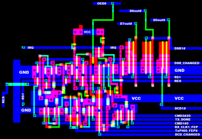
7a) Status register, Bit 7..5

When reading it:
ST7=1 indicates an active interrupt, means that the low_active IRQ# pad is pulled LOW by the 8551.
ST6 gives you what's on the DSR# pad //see "5b) DSR#"
ST5 gives you what's on the DCD# pad //see "5c) DCD#"

Bit 5 and Bit 6 are trivial, so we now focus on Bit 7:

;...

First the TX interrupt:

High active signal TX_DONE, synchronized with TxPHI0_FEP# clock,
goes together with control signal CMD3#20 into an AND gate.
The output of said AND gate basically is the TX interrupt,
which hits after a transmission is done.

TX_DONE is generated in "17) TX control".
TxPHI0_FEP# is generated in "19) TX div16". //TX clock predivider.

CMD3#20 is generated in "12) Control/Command register output decoding".
It is HIGH when CMD3=0 AND CMD2=1 AND CMD0=1.
//TX interrupt enabled, RTS#=LOW, transmitter enabled.

;...

Second the RX interrupt:

High_active signal RX_CLK1_FEP, which is generated in "18) RX div16", //the RX clock predivider
indicates the end of a RX sequence.
It goes together with control signal CMD1#0 into another AND gate.
The output of said AND gate basically is the RX interrupt.

CMD1#0 is generated in "12) Control/Command register output decoding".
It is HIGH when CMD1=0 AND CMD0=1.
//RX interrupt enabled, receiver enabled.

;...

We have two RS flipflops:
First the "RX/TX IRQ sample FF", which samples the RX/TX interrupt.
Second the "RX/TX IRQ FF", which actually is the RS/TX interrupt flag.

RX interrupt and TX interrupt go into an OR gate.
The output of the OR gate sets the "RX/TX IRQ sample FF".

If no Status register read is in progress:
"RX/TX IRQ sample FF" sets "RX/TX IRQ FF".
After "RX/TX IRQ FF" went set, "RX/TX IRQ sample FF" is cleared.

A status register read clears "RX/TX IRQ FF", blocks "RX/TX IRQ FF" set,
and blocks "RX/TX IRQ sample FF" clear.

A hardware reset with RES active also clears "RX/TX IRQ FF".

;...

High_active signal DSR_CHANGED indicates that the logic level at the DSR# pad has changed
from LOW to HIGH (or from HIGH to LOW) since the last Status register read.
It is generated in "5b) DSR#".

High_active signal DCD_CHANGED indicates that the logic level at the DCD# pad has changed
from LOW to HIGH (or from HIGH to LOW) since the last Status register read.
It is generated in "5c) DCD#".

The high_active Q output of "RX/TX IRQ FF", DSR_CHANGED and DCD_CHANGED go into an OR gate.
The output of said OR gate is sampled by a half_static transparent latch
when no Status register read is in progress.

The output of that latch is the IRQ signal which goes to the "2e) IRQ#" pad driver,
and IRQ what you see in Bit 7 when reading the Status register.

;---

Note, that PHI2, RX clock and TX clock are different clock domains.

8552 makes creative use of RS flipflops for getting a signal from one domain to the other.

Problem is:
If you are out to do a 8551 FPGA implementation, you won't have RS flipflops.
You probably even would have no transparent latches, but only edge triggered flipflops.
And for the IDE... if you just insert one logic gate into a clock signal path,
the IDE stubbornly will insist that you have two different clock domains at the input and the output,
and it will tread circuitry clocked by the two domains like they happen to be located on two different planets.
So be warned, that you might be getting some more grey hairs there.

Oh, and for a lot of the RS flipflops inside the 8551,
correct functionality of the circuitry depends on the priority for R,S inputs to Q,/Q outputs,
take care.

;---

Attachment:
si8551r2_7a_stat_reg_7_5.png
si8551r2_7a_stat_reg_7_5.png [ 22.07 KiB | Viewed 424 times ]

Attachment:
8551r2_7a_stat_reg_7_5.png
8551r2_7a_stat_reg_7_5.png [ 95.24 KiB | Viewed 424 times ]


Top
 Profile  
Reply with quote  
PostPosted: Fri Mar 17, 2023 8:53 am 
Offline
User avatar

Joined: Fri Nov 09, 2012 5:54 pm
Posts: 1397
7b) Status register, Bit 4..2

ST4=1 indicates, that the transmitter data register is empty.

High_active signal DataReg>TX (which is generated in "17) TX control")
loads the TX shift register with the contents of the TX data register.

We have two RS flipflops.
The first RS flipflop samples the "TX data register went empty" condition,
the second RS flipflop actually is the ST4 "TX data register not empty" flag.

DataReg>TX sets the first RS flipflop.
After the first RS flipflop went set,
a falling edge on DataReg>TX will clear the ST4 flag RS flipflop.
If the ST4 flag RS flipflop is cleared, it will clear the first RS flipflop.

A hardware reset with RES active also clears the ST4 flag RS flipflop.

The "7d" edge detector generates a pulse on the high_active TX_DRW signal
at the falling edge of W$0 (the end of a TX data register write by the CPU).

The ST4 flag RS flipflop has a non_inverting output Q which goes into an inverter,
said inverter generates the low_active TDR_NE# signal,
which indicates that the TX data register is not empty.
TDR_NE# goes into "17) TX control".

The ST4 flag RS flipflop has an inverting output /Q,
which is sampled by a half_static transparent latch when no Status register read is in progress.
The inverted output of said latch is what you see in Bit 4 when reading the Status register.

Again:
correct functionality of the circuitry depends on the priority for R,S inputs to Q,/Q outputs,
take care.

;---

ST3=1 indicates, that the receiver data register is full.

High_active signal RX_CLK1_FEP, which is generated in "18) RX div16", //the RX clock predivider
indicates the end of a RX sequence.
It sets the ST3 flag RS flipflop.

A receiver data register read by the CPU clears the ST3 flag RS flipflop.
A hardware reset with RES active also clears the ST3 flag RS flipflop.

The ST3 flag RS flipflop has an inverting output /Q which goes into an inverter,
said inverter generates the high_active signal RDR_FULL,
which indicates that the receiver data register is full.
RDR_FULL goes into the Status register Bit 3 circuitry for detecting RX overrun.
RDR_FULL also goes into "8c RX data register input" for blocking
subsequent transfers of the RX shift register contents into the RX data register
in case of RX overrun.

The ST3 flag RS flipflop has a non_inverting output Q,
which is sampled by a half_static transparent latch when no Status register read is in progress.
The inverted output of said latch is what you see in Bit 3 when reading the Status register.

Again:
correct functionality of the circuitry depends on the priority for R,S inputs to Q,/Q outputs,
take care.

;---

ST2=1 indicates RX overrun, and ST2 changes with every received frame.

RDR_FULL is sampled with a half_static transparent latch when RX_CLK1=1
(when the 8551 wants to transfer the contents of the RX shift register
into the RX data register, that is).

The latch is cleared with high_active register write control signal signal W$1,
that's when the CPU does a programmed reset of the 8551 by writing to the Status register.
A hardware reset with RES active also clears the latch.

The output of that latch is what you see in Bit 2 when reading the status register.

;---

Attachment:
si8551r2_7b_stat_reg_4_2.png
si8551r2_7b_stat_reg_4_2.png [ 19.18 KiB | Viewed 424 times ]

Attachment:
8551r2_7b_stat_reg_4_2.png
8551r2_7b_stat_reg_4_2.png [ 89.54 KiB | Viewed 424 times ]


Top
 Profile  
Reply with quote  
PostPosted: Fri Mar 17, 2023 8:54 am 
Offline
User avatar

Joined: Fri Nov 09, 2012 5:54 pm
Posts: 1397
7c) Status register, Bit 1..0

ST1=1 indicates that a RX framing error was detected, and ST1 changes with every received frame.

RXDin# is the inverted signal from the RXD pad. //see "4e) RXD"
;
When there is supposed to be a Stopbit, which is supposed to be HIGH,
the RXD pad is supposed to be high, and RXDin# is supposed to be LOW.

The high_active FERR signal, which is generated in "14) RX control",
indicates that the additional Stopbit was not HIGH (when we have more than one Stopbit).

High_active signal RX>DataReg loads the contents of the RX shift register
into the RX data register.
//I think this is supposed ot happen while receiving the last Stopbit.

RXDin# and FERR go into an OR gate.
A half_static transparent latch samples the output of said OR gate when RX>DataReg is HIGH.
A hardware reset with RES active clears the latch.

The output of said latch is what you see in Bit 1 when reading the Status register.

;---

ST0=1 indicates that a RX parity error was detected, and ST0 changes with every received frame.

CMD7=0 means that Parity is enabled.
CMD5=1 means that Parity check is enabled. //when Parity is enabled

CMD_7 is the buffered output of CMD7, Command register Bit 7.
CMD_5# is the inverted output of CMD5, Command register Bit 5.
Both signals are generated in "12) Control/Command register output decoding".

Low_active signal PERR# is generated in "14) RX control".
When PERR# is LOW, this indicates that something was wrong with the parity of the received frame.

CMD_7, CMD_5# and PERR# go into a NOR gate.
A half_static transparent latch samples the output of said OR gate when RX>DataReg is HIGH.
A hardware reset with RES active clears the latch.

The output of said latch is what you see in Bit 0 when reading the Status register.

;---

Attachment:
si8551r2_7c_stat_reg_1_0.png
si8551r2_7c_stat_reg_1_0.png [ 12.53 KiB | Viewed 424 times ]

Attachment:
8551r2_7c_stat_reg_1_0.png
8551r2_7c_stat_reg_1_0.png [ 48.25 KiB | Viewed 424 times ]


Top
 Profile  
Reply with quote  
PostPosted: Fri Mar 17, 2023 8:55 am 
Offline
User avatar

Joined: Fri Nov 09, 2012 5:54 pm
Posts: 1397
7d) W$0 edge detector

Nothing special.

It's just a falling edge detector, making use of the gate delay of inverters.

When the CPU writes the TX data register,
high_active register write control signal W$0 is HIGH.

The edge detector scans for the falling edge of W$0,
that's the end of the write.
It then generates a short HIGH pulse on signal TX_DRW.

Signal TX_DRW goes into the "7b) Status register, Bit 4" circuitry.

Attachment:
si8551r2_7d_stat_reg_edge_det.png
si8551r2_7d_stat_reg_edge_det.png [ 7.34 KiB | Viewed 424 times ]

Attachment:
8551r2_7d_stat_reg_edge_det.png
8551r2_7d_stat_reg_edge_det.png [ 16.77 KiB | Viewed 424 times ]


Top
 Profile  
Reply with quote  
PostPosted: Fri Mar 17, 2023 8:57 am 
Offline
User avatar

Joined: Fri Nov 09, 2012 5:54 pm
Posts: 1397
8) RX data register //plus RX shift register

Attachment:
8551r2_8_rx_data_register.png
8551r2_8_rx_data_register.png [ 26.36 KiB | Viewed 424 times ]


;---

Thing is, that the shift register is built from master/slave flipflops,
each master/slave flipflop contains two half_static latches.

This means something like a four phase non_overlapping clock...
...inside a 65xx chip.

My guess is that the designer wasn't just "a bit paranoid" about the clock LOW/HIGH time,
but maybe about the clock rise/fall time too.

It doesn't look bad _now_, when dissecting the RX and TX shift registers.
But the Bitcounters related to both shift registers and the predividers
for the RX and TX clock use that sort of master/slave flipflops too.

If you are trying to go down the rabbit hole of how that circuitry works at transistor level,
be warned that it might not be a healthy thing to do.


Top
 Profile  
Reply with quote  
PostPosted: Fri Mar 17, 2023 8:58 am 
Offline
User avatar

Joined: Fri Nov 09, 2012 5:54 pm
Posts: 1397
8a) RX data register (plus RX shift register), Bit 7

While dissecting the silicon, I went from West to East,
and that's why I took a look at Bit 7 first.
//LSB is shifted in first.

When ignoring the hold paths of the half_static latches,
the circuitry actually become more understandable.
Means, we are ignoring the shift register clock signals RxPHI1N and RxPHI2N.

First we have one Bit of the RX shift register, built from a master/slave flipflop,
which contains two half_static latches.

The clock signals for the RX shift register are:
RxPHI1 (RxPHI1N is inverted RxPHI1),
RxPHI2 (RxPHI2N is inverted RxPHI2).
Said clock signals are generated in "15) RX Bitcounter".

The RX Bitcounter uses a ring counter which is built from a similar shift register,
so using the same clock signals for the RX shift register and the RX Bitcounter
makes a lot of sense.

RXDin# is the low_active serial data input,
which is generated by an inverter which is fed by the RXD pad. //see "4e) RXD".
;
In "8c)", RXDin# goes through another inverter and becomes high_active RX_Din.

The serial input of the RX Bit 7 shift register is fed by RX_Din.

Since the 8551 supports 5..8 Bit data length,
we have a 2:1 multiplexer which feeds the serial input of the Bit 6 RX shift register with:
L7#=0: serial output of the Bit 7 RX shift register
L7#=1: RX_Din, what bypasses Bit 7 of the RX shift register

Also, L7#=1 clears the RxPHI1 latch of the shift register.

;...

Attached to the output of the 2:1 multiplexer,
we have a half_static transparent latch,
which is Bit 7 of the RX data register.
L7#=1 clears this latch.

The latch is loaded when high_active RX>DataReg signal is HIGH.
RX>DataReg is generated in "8c)".

Because it's a half_static latch, we also have the low_active
RX>DataReg# signal, which is generated in "8c)" too.

;---

Bit 6 and Bit 5 circuitry is pretty similar.

L7#=1 bypasses RX shift register Bit 7
L6#=1 bypasses RX shift register Bits 7,6
L5#=1 bypasses RX shift register Bits 7,6,5

L7#, L6#, L5# signals are generated in "12) Control/Command register output decoding".

L7#=0 AND L6#=0 AND L5#=0: 8 Bit data size
L7#=1 AND L6#=0 AND L5#=0: 7 Bit data size
L7#=1 AND L6#=1 AND L5#=0: 6 Bit data size
L7#=1 AND L6#=1 AND L5#=1: 5 Bit data size

;---

Attachment:
si8551r2_8a_rx_data_register_7.png
si8551r2_8a_rx_data_register_7.png [ 13.13 KiB | Viewed 423 times ]

Attachment:
8551r2_8a_rx_data_register_7.png
8551r2_8a_rx_data_register_7.png [ 55.72 KiB | Viewed 423 times ]


Top
 Profile  
Reply with quote  
PostPosted: Fri Mar 17, 2023 8:59 am 
Offline
User avatar

Joined: Fri Nov 09, 2012 5:54 pm
Posts: 1397
8b) RX data register (plus RX shift register), Bit 4

Pretty much the same circuitry we had in "8a)" with Bit 7..5,
except that there is no 2:1 multiplexer,
and that the data register latch isn't cleared.

The chip layout for Bit 4..0 is pretty much identical.

Attachment:
si8551r2_8b_rx_data_register_4.png
si8551r2_8b_rx_data_register_4.png [ 11.7 KiB | Viewed 423 times ]

Attachment:
8551r2_8b_rx_data_register_4.png
8551r2_8b_rx_data_register_4.png [ 45.81 KiB | Viewed 423 times ]


Top
 Profile  
Reply with quote  
PostPosted: Fri Mar 17, 2023 9:00 am 
Offline
User avatar

Joined: Fri Nov 09, 2012 5:54 pm
Posts: 1397
8c) RX data register (plus shift register) serial input

Serial data goes in LSB first.
But in the chip layout, the circuitry for the serial input
of the RX shift rgister is East of RX shift register Bit 0.
It sends serial data into RX shift register Bit 7..5,
so don't please don't get confused by how things are arranged in the silicon.

What we have when ignoring the hold path of the half_static latches:

High_active signal RX_CLK1 (which is generated in "18) RX div 16", the RX CLK predivider)
indicates the last Stopbit of a frame.
It goes into an inverter, which gives out the low_active signal RX_CLK1#.

High_active signal RDR_FULL indicates that the RX data register already is full,
it is generated in "7b) Status register, Bit 3".

RX_CLK1# and RDR_FULL go into an OR gate, which gives out the high_active signal RX>DataReg.
Means, that if the RX shift register has new data to be loaded into the RX data register,
and the RX data register still is not empty (not ready to take the new data),
the new data is not loaded into the RX data register, and we are heading toward OVERRUN condition.

RX>DataReg goes into an inverter which generates the low_active signal RX>DataReg#.

RX>DataReg and RX>DataReg# go into "8a)" and "8b)" for controlling the latches
of the RX data register.

;...

RXDin# is the low_active serial data input,
which is generated by an inverter which is fed by the RXD pad. //see "4e) RXD".
;
RXDin# goes through an inverter and becomes high_active RX_Din.
RX_Din then goes into "8a)" RX shift register Bit 7..5.

Attachment:
si8551r2_8c_rx_data_register_input.png
si8551r2_8c_rx_data_register_input.png [ 12.56 KiB | Viewed 423 times ]

Attachment:
8551r2_8c_data_register_input.png
8551r2_8c_data_register_input.png [ 27.11 KiB | Viewed 423 times ]


Top
 Profile  
Reply with quote  
PostPosted: Fri Mar 17, 2023 9:01 am 
Offline
User avatar

Joined: Fri Nov 09, 2012 5:54 pm
Posts: 1397
9) TX data register //plus TX shift register

Attachment:
8551r2_9_tx_data_register.png
8551r2_9_tx_data_register.png [ 25.81 KiB | Viewed 423 times ]


;---

And yes:
Shift register is built from master/slave flipflops,
each master/slave flipflop contains two half_static latches.
...Again.


Top
 Profile  
Reply with quote  
PostPosted: Fri Mar 17, 2023 9:03 am 
Offline
User avatar

Joined: Fri Nov 09, 2012 5:54 pm
Posts: 1397
9a) TX data register (plus TX shift register)

Circuitry for Bit 0..7 looks pretty much the same,
except that we have an additional transistor for Bit 7,
same thing for Bit 6 and Bit 5.

So let's just ignore the hold paths of the half_static latches,
and focus on Bit 7.

First we have a half_static transparent latch, which is the TX Bit 7 data register.
The CPU writes data into it with high_active register write control signal W$0=HIGH.

High_active W$0 and low_active W$0# are generated in "6) address decoder".

Signal L7#=1 clears the latch. //That's the additional transistor for Bit 7.
Since the write data bus line D7in# which goes into the latch is low_active,
L7#=1 actually _sets_ TX data register Bit 7.

The 8551 supports data lengths of 5..8 Bits,
for data lengths of less than 8 Bits the unused Bits in the TX data registers are set to 1
with the L7#, L6#, L5# signals.
For more info about these signals, see "8a) RX data register (plus shift register), Bit 7..5".

;...

We have one Bit of the TX shift register, built from a master/slave flipflop
which contains two half_static transparent latches.

When high_active signal DataReg>TX is HIGH, the contents of the TX data register
are asynchronously loaded into the TxPHI2 latch of the TX shift register.
Signal DataReg>TX is generated in "17) TX control".

Data is shifted out LSB first,
the serial input of TX shift register Bit 7 is tied to HIGH.

High_active signal TX_SR_HI=HIGH asynchronously sets all of the TxPHI1 latches
in the TX shift register, it is generated in "17) TX control".

The clock signals for the TX shift register are:
TxPHI1 (TxPHI1N is inverted TxPHI1),
TxPHI2 (TxPHI2N is inverted TxPHI2).
Said clock signals are generated in "16) TX Bitcounter".

The TX Bitcounter uses a ring counter which is built from a similar shift register,
so using the same clock signals for the TX shift register and the TX Bitcounter
makes a lot of sense.

Attachment:
si8551r2_9a_tx_data_register_7.png
si8551r2_9a_tx_data_register_7.png [ 15.82 KiB | Viewed 423 times ]

Attachment:
si8551r2_9a_tx_data_register_4.png
si8551r2_9a_tx_data_register_4.png [ 13.8 KiB | Viewed 423 times ]

Attachment:
8551r2_9a_tx_data_register.png
8551r2_9a_tx_data_register.png [ 53.62 KiB | Viewed 423 times ]


Top
 Profile  
Reply with quote  
PostPosted: Fri Mar 17, 2023 9:04 am 
Offline
User avatar

Joined: Fri Nov 09, 2012 5:54 pm
Posts: 1397
9b) TX data register (plus TX shift register) output

TX serial data is shifted out LSB first.
But before the first data Bit goes out, the Startbit goes out.

That's why we have another Bit of TX shift register containing the Startbit,
the serial input is fed by the serial output of the TX shift register LSB.

Said TX shift register Bit isn't different from the TX shift register Bits
we already had in "9a", including the control signals.

Except that the control signal DataReg>TX (which transfers the contents of the
TX data register into the TX shift register) transfers 0 into the TxPHI2 latch,
because the Startbit has to be 0.

The output of the TX shift register Startbit flipflop goes into an inverter,
which sends the low_active TX shift register output TX_Q# into "17) TX control",
which controls the TXD pad driver, and that's all.

Attachment:
si8551r2_9b_tx_data_register_output.png
si8551r2_9b_tx_data_register_output.png [ 11.95 KiB | Viewed 423 times ]

Attachment:
8551r2_9b_tx_data_register_output.png
8551r2_9b_tx_data_register_output.png [ 44.71 KiB | Viewed 423 times ]


Top
 Profile  
Reply with quote  
Display posts from previous:  Sort by  
Post new topic Reply to topic  [ 45 posts ]  Go to page Previous  1, 2, 3  Next

All times are UTC


Who is online

Users browsing this forum: Google [Bot] and 59 guests


You cannot post new topics in this forum
You cannot reply to topics in this forum
You cannot edit your posts in this forum
You cannot delete your posts in this forum
You cannot post attachments in this forum

Search for:
Jump to: