6502.org Forum  Projects  Code  Documents  Tools  Forum
It is currently Fri Jun 28, 2024 3:07 pm

All times are UTC


Post new topic Reply to topic  [ 26 posts ]  Go to page Previous  1, 2
Author Message
 Post subject:
PostPosted: Thu Aug 05, 2010 11:26 am 
Offline

Joined: Mon Mar 02, 2009 7:27 pm
Posts: 3258
Location: NC, USA
"star" distribution, i.e. from the center outwards. I use this principle when wire-wrapping power connections.

More recently, I've been applying this principle to data bus and address lines too. Am I correct in doing so?

_________________
65Org16:https://github.com/ElEctric-EyE/verilog-6502


Top
 Profile  
Reply with quote  
 Post subject:
PostPosted: Thu Aug 05, 2010 7:57 pm 
Offline

Joined: Tue Jul 05, 2005 7:08 pm
Posts: 1017
Location: near Heidelberg, Germany
It seems that fixing the power supply on the CPU board has fixed my problem! Yesterday it ran for over an hour already, and it's been running for almost an hour now without issue.

It always amazes me. A power supply issue on the CPU board with its drivers only makes a difference if on the BIOS board a larger RAM is used...

Pity that it's a a lesson already learned - I'm doing a much better board design concerning power supply these days than I did then. So it's a sin of the past that seems to have haunted me here... ;-)

BTW: the replacement RAMs I ordered, although the datasheet on the web site said something different, are of the very same type again....

Thanks for your help folks - sometimes it's enough just to discuss a problem to get on the right track.

André


Top
 Profile  
Reply with quote  
 Post subject:
PostPosted: Thu Aug 05, 2010 8:02 pm 
Offline

Joined: Tue Jul 05, 2005 7:08 pm
Posts: 1017
Location: near Heidelberg, Germany
ElEctric_EyE wrote:
"star" distribution, i.e. from the center outwards. I use this principle when wire-wrapping power connections.

More recently, I've been applying this principle to data bus and address lines too. Am I correct in doing so?


I'm not sure about that. Would you not get signal reflections on all the ends of the "rays" that then add up in the middle again?

When going to higher frequencies (or DRAMs :-) I am now more inclined to actually do some bus design: single signal line, feed from one side through small series resistor, terminator resistors, and only very short connects from this bus line to each receiver.

Maybe "star distribution" works with appropriate termination on each of the rays, and maybe even series resistors at the beginning of each ray (making it a variation of my "bus design".)

But others here are more experienced in these matters than I am :-)

André


Top
 Profile  
Reply with quote  
 Post subject:
PostPosted: Thu Aug 05, 2010 9:11 pm 
Offline
User avatar

Joined: Fri Aug 30, 2002 1:09 am
Posts: 8460
Location: Southern California
I can't see stars being practical at all for more than power and ground. Even for just that, the wires are piled kind of thick in the middle.


Top
 Profile  
Reply with quote  
 Post subject:
PostPosted: Fri Aug 06, 2010 12:52 am 
Offline

Joined: Mon Mar 02, 2009 7:27 pm
Posts: 3258
Location: NC, USA
Glad to hear you fixed the problem! Heh, a solution to problem revisited is almost never forgotten.

In the past, when wiring data and address connections between CPU, SRAM, EPPROM and peripherals, I used to hop from CPU, to SRAM, to EPROM, etc., i.e. "tree" distribution. Now I wirewrap power, data, and address from CPU to SRAM, CPU to EEPROM, etc. Common sense tells you if you can keep all these IC's around the CPU, the distances would be shorter, but... Andre picked up on something here. I too am unfamiliar with electromagnetic workings inside the wire, skin effect, reflections, etc. I ask now because soon I will have to have PCBs made, very soon. I would like to get it right the first time. This could be a good thread to continue this topic?

_________________
65Org16:https://github.com/ElEctric-EyE/verilog-6502


Top
 Profile  
Reply with quote  
 Post subject:
PostPosted: Fri Aug 06, 2010 2:40 am 
Offline
User avatar

Joined: Thu May 28, 2009 9:46 pm
Posts: 8234
Location: Midwestern USA
ElEctric_EyE wrote:
In the past, when wiring data and address connections between CPU, SRAM, EPPROM and peripherals, I used to hop from CPU, to SRAM, to EPROM, etc., i.e. "tree" distribution. Now I wirewrap power, data, and address from CPU to SRAM, CPU to EEPROM, etc. Common sense tells you if you can keep all these IC's around the CPU, the distances would be shorter, but... Andre picked up on something here. I too am unfamiliar with electromagnetic workings inside the wire, skin effect, reflections, etc. I ask now because soon I will have to have PCBs made, very soon. I would like to get it right the first time. This could be a good thread to continue this topic?

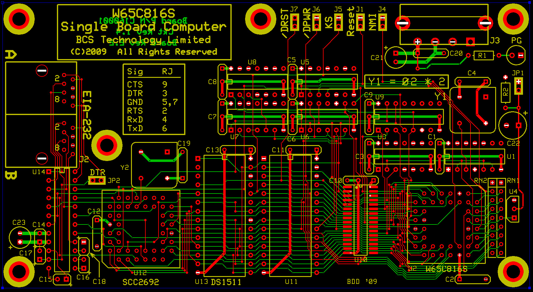
When I was doing the POC layout I first looked at the idea of the MPU being in the middle and everything kind of fanning out from there. However, it soon became apparent that doing so would actually increase the aggregate length of the bus traces, the opposite of what was wanted.

After several iterations of the design, I came up with a layout in which the SRAM was immediately to the left of the MPU (which is in a PLC44 socket), the EPROM to the left of the SRAM, the watchdog timer to the left of the EPROM and the DUART to the left of the watchdog. The reasoning behind this is the SRAM is connected A0-A15, the EPROM to A0-A12, the watchdog to A0-A4 and the DUART to A0-A3. This arrangement makes more sense when you also consider that all of the decoding logic is attached to the higher addresses, thus adding some length to those lines. To minimize the trace lengths to the decoding logic, I placed those ICs immediately above the MPU.

In all likelihood, I was overcautious with my layout, as PC motherboards seem to be able to get away with some pretty long traces to the PCI sockets, all of which operate at 33 MHz (much higher for PCI-X and PCI-E). I also used a four-layer board, both to improve noise and layer crosstalk immunity, and to not have to route individual power and ground traces everywhere.

POC V1.0 Printed Circuit Board

_________________
x86?  We ain't got no x86.  We don't NEED no stinking x86!


Top
 Profile  
Reply with quote  
 Post subject:
PostPosted: Fri Aug 06, 2010 2:44 am 
Offline
User avatar

Joined: Thu May 28, 2009 9:46 pm
Posts: 8234
Location: Midwestern USA
fachat wrote:
It seems that fixing the power supply on the CPU board has fixed my problem! Yesterday it ran for over an hour already, and it's been running for almost an hour now without issue.

I can't say that I'm surprised. An automobile is no better than the quality of the fuel in its tank, and a computer only runs as well as the power supply will let it.

_________________
x86?  We ain't got no x86.  We don't NEED no stinking x86!


Top
 Profile  
Reply with quote  
 Post subject:
PostPosted: Fri Aug 06, 2010 3:07 am 
Offline
User avatar

Joined: Fri Aug 30, 2002 9:02 pm
Posts: 1696
Location: Sacramento, CA
BigDumbDinosaur wrote:
I also used a four-layer board, both to improve noise and layer crosstalk immunity, and to not have to route individual power and ground traces everywhere.

POC V1.0 Printed Circuit Board


I have a question for you concerning the bypass capacitors on your layout. I too have plans for a high-speed 65816-based system that would use the ExpressPCB 4-layer boards. In my design, I placed the caps like you did (near the Vcc pin), but I planned on having the caps legs connected directly to the respective power and ground layers. In your design, you bring the ground pin connection from the DIP IC's to the cap's using a thick surface trace. Also, you did the PLCC devices' caps directly to the power/ground planes.

Can you share your reasoning for doing it this way as my education in this area is quite lacking. I must say you layed your board out very nicely and I can appreciate the time you took to optimize it.

Daryl


Top
 Profile  
Reply with quote  
 Post subject: Bypassing
PostPosted: Fri Aug 06, 2010 5:57 am 
Offline
User avatar

Joined: Thu May 28, 2009 9:46 pm
Posts: 8234
Location: Midwestern USA
8BIT wrote:
I have a question for you concerning the bypass capacitors on your layout. I too have plans for a high-speed 65816-based system that would use the ExpressPCB 4-layer boards. In my design, I placed the caps like you did (near the Vcc pin), but I planned on having the caps legs connected directly to the respective power and ground layers. In your design, you bring the ground pin connection from the DIP IC's to the cap's using a thick surface trace. Also, you did the PLCC devices' caps directly to the power/ground planes.

Can you share your reasoning for doing it this way as my education in this area is quite lacking. I must say you layed your board out very nicely and I can appreciate the time you took to optimize it.

Daryl

The idea behind tying the Vcc end of each bypass capacitor directly to its associated device pin is make sure a given cap doesn't act as a bypass for other devices. The theory behind this is based on the propagation time of the high frequency noise generated by the chip switching transients. If the bypass cap for a given chip is not connected directly to that chip's Vcc, then the transient noise must go out onto the power path (traces or inner layer) to get to the cap. This would allow the energy in the transient to spread to other parts of the circuit, with undefined effects. If the connection from Vcc to the cap is short and heavy, this spreading effect is greatly diminished and the bypass cap does a much better job.

As for the PLCC devices (MPU and DUART), I did directly connect each bypass cap to the associated device's Vcc pin. However, owing to the 100 mil grid layout used by the sockets, it wasn't practical to tie the device's ground pin to the bypass cap. This is not any particular disadvantage, due to the large area of the internal ground layer.

I have since determined from when I did the POC layout that the direct connection of the bypass cap to the device's ground terminal doesn't produce any significant improvement in noise suppression (based on 'scope observations). You will be okay in connecting your bypass caps directly to ground. However, I recommend the short and heavy direct connection between the device's Vcc pin and the bypass cap.

Incidentally, the bypass caps on my POC design are AVX SR275E104MAA multilayer ceramics, 0.1 mf at 50 volts. They are readily available from Mouser and others.

Also, I've developed a new board layout for POC 2.0, which includes an expansion port so I can test my yet-to-be-built SCSI host adapter. I'll put up a link to its picture when available.

_________________
x86?  We ain't got no x86.  We don't NEED no stinking x86!


Top
 Profile  
Reply with quote  
 Post subject:
PostPosted: Fri Aug 06, 2010 12:19 pm 
Offline
User avatar

Joined: Fri Aug 30, 2002 9:02 pm
Posts: 1696
Location: Sacramento, CA
Thanks for the explanations. I will adjust my layout accordingly.

Daryl


Top
 Profile  
Reply with quote  
 Post subject: Re: Bypassing
PostPosted: Sat Aug 07, 2010 4:18 am 
Offline
User avatar

Joined: Thu May 28, 2009 9:46 pm
Posts: 8234
Location: Midwestern USA
BigDumbDinosaur wrote:
Also, I've developed a new board layout for POC 2.0, which includes an expansion port so I can test my yet-to-be-built SCSI host adapter. I'll put up a link to its picture when available.

I posted a link to the new PCB layout under the POC topic.

_________________
x86?  We ain't got no x86.  We don't NEED no stinking x86!


Top
 Profile  
Reply with quote  
Display posts from previous:  Sort by  
Post new topic Reply to topic  [ 26 posts ]  Go to page Previous  1, 2

All times are UTC


Who is online

Users browsing this forum: No registered users and 5 guests


You cannot post new topics in this forum
You cannot reply to topics in this forum
You cannot edit your posts in this forum
You cannot delete your posts in this forum
You cannot post attachments in this forum

Search for:
Jump to: