6502.org Forum  Projects  Code  Documents  Tools  Forum
It is currently Fri Sep 20, 2024 7:17 pm

All times are UTC


Post new topic Reply to topic  [ 48 posts ]  Go to page 1, 2, 3, 4  Next
Author Message
 Post subject: Re: Speed & EEPROMs
PostPosted: Thu Jun 18, 2015 5:20 am 
Offline
User avatar

Joined: Fri Dec 11, 2009 3:50 pm
Posts: 3367
Location: Ontario, Canada
cbscpe wrote:
You could use a dual-rate clock. After a reset the CPU runs at half the speed and the ROM region really selects the ROM. The reset routine copies the ROM to the RAM which overlays the ROM.
The ROM-to-RAM copy approach has some interesting advantages. But sometimes we want to "just make the darn EPROM work"! -- using the simplest means possible. :?


Generating wait states:
Attachment:
simple wait-state generator.gif
simple wait-state generator.gif [ 4 KiB | Viewed 9052 times ]
The circuit above generates a one-cycle-long wait state when the EPROM is accessed. (For WDC, it's best to add a series resistor -- see below.) One wait state may not sound like much; but, when you're pushing the CPU close to its maximum clock rate, adding one wait-state roughly triples the time available for the EPROM to respond! Here's why. At high clock rates tADS and tDSR delays (which each consume a fixed number of nanoseconds) end up accounting for about 50% of all the nanoseconds in a clock cycle. (65xx timing is graphically explained in the Visual Guide to 65xx CPU Timing).

The access time remaining for memory to do its job works out to roughly 50% of the nanoseconds in one clock cycle. Adding a one-cycle-long wait state changes this figure from 50% to 150%. (The tADS and tDSU delays don't get applied again when a wait-state cycle is inserted.) Stated another way, if the cycle time is 100 ns, say, then adding a one-cyle-long wait state increases the available memory access time by 100 ns.

-- Jeff

ETA: There's an implicit assumption. The circuit only works if /CS goes low before the rise of Ø2 -- which is normally the case. BDD touches on this in the following post. Also: using the both halves of the '109, two wait states can be provided (see circuit below). The extra access time thus provided will be 200% of one cycle. The total access time will be about 5 times what's available using no wait states.
Attachment:
double-wait-state generator.gif
double-wait-state generator.gif [ 4.32 KiB | Viewed 9039 times ]


Further edit: in contrast to Rockwell and other suppliers, WDC makes the RDY pin bi-directional. A WDC 'C02 or '816 will pull its own RDY pin low as a result of executing a WAI instruction. This can result in excessive current flow if the RDY pin is driven high by external logic at the same time.

One solution is to use an Open-Collector or Open-Drain gate to drive RDY (as shown in the upper diagram in image below) but this limits the ability for RDY to quickly return high. It's better to use an ordinary gate and simply include a series resistor to limit current flow (lower diagram).

WDC's datasheet was revised to include a comment about the series resistor (as well as a comment about pullup resistors).
Attachment:
bi-directional RDY - WDC caveat.gif
bi-directional RDY - WDC caveat.gif [ 12.97 KiB | Viewed 8807 times ]

Unfortunately WDC doesn't suggest a value for the series resistor, so let's look at that question. Too low a value means increased dissipation, and the risk that a valid logic-low voltage won't be achieved. OTOH too high a value will produce unacceptable delay re the RC of the gate and resistor driving the capacitance of the RDY input. I myself would use a series resistor of around 470 ohms -- a rather low value, but IMO not so low as to prevent a valid logic-low voltage from being achieved. In another thread Garth suggests putting a small (~22 pF) capacitor in parallel with the resistor, which allows use of a much higher resistance but of course increases the component count slightly.
Attachment:
bi-directional RDY re WDC 02 and 816.gif
bi-directional RDY re WDC 02 and 816.gif [ 9.15 KiB | Viewed 8904 times ]

_________________
In 1988 my 65C02 got six new registers and 44 new full-speed instructions!
https://laughtonelectronics.com/Arcana/ ... mmary.html


Last edited by Dr Jefyll on Sat Nov 28, 2015 3:12 pm, edited 5 times in total.

Top
 Profile  
Reply with quote  
 Post subject: Re: Speed & EEPROMs
PostPosted: Thu Jun 18, 2015 5:48 am 
Offline
User avatar

Joined: Thu May 28, 2009 9:46 pm
Posts: 8390
Location: Midwestern USA
banedon wrote:
Thanks for the responses, guys.
The circuit diagram is attached below...

Something I noted is that it appears that you are gating the SRAM chip select with Ø2. That is generally not good practice. The problem as it stands is that the SRAM will not respond to chip select until sometime after Ø2 has gone high, which will set a hard limit on performance. It's better to select the SRAM (and ROM) as soon as a valid address appears on the bus, which is early during Ø2 low, and then gate /OE or /WE on the rise of Ø2. That way, all of the Ø2 high period is available to read or write.

Also, many SRAMs respond faster to /OE and /WE than to /CS. So the procedure I recommend (and use in POC) is to assert /CS as soon as the address is valid and then assert /OE or /WE only when Ø2 rises. As an example, the SRAM I'm using in POC V1.1 is guaranteed to respond to /CS in 12ns or less. If /CS is already asserted and /OE is then asserted, the SRAM will drive the data bus in 6ns or less. If /OE is already asserted and /CS is used to gate the device the elapsed time until the SRAM starts driving D0-D7 is 12ns.

I also saw a mention of the using the clock outputs of the 65C02 to drive all the other devices that need to know about the clock, and only driving the 65C02 from the Ø2 clock generator. Here's what WDC has to say about it:

    3.8 Phase 2 In (PHI2), Phase 2 Out (PHI2O) and Phase 1 Out (PHI1O)

    Phase 2 In (PHI2) is the system clock input to the microprocessor internal clock. During the low power Standby Mode, PHI2 can be held in either high or low state to preserve the contents of internal registers since the microprocessor is a fully static design. The Phase 2 Out (PHI2O) signal is generated from PHI2. Phase 1 Out (PHI1O) is the inverted PHI2 signal. An external oscillator is recommended for driving PHI2 and used for the main system clock. All production test timing is based on PHI2. PHI2O and PHI1O were used in older systems for system timing and internal oscillators when an external crystal was used.

In other words, WDC does not recommend the use of PHIO1 and PHIO2 in new designs. You should also consider the fact that PHI1O and PHI2O lag Ø2 by an amount that is not specified.

_________________
x86?  We ain't got no x86.  We don't NEED no stinking x86!


Top
 Profile  
Reply with quote  
 Post subject: Re: Speed & EEPROMs
PostPosted: Thu Jun 18, 2015 5:55 am 
Offline
User avatar

Joined: Thu May 28, 2009 9:46 pm
Posts: 8390
Location: Midwestern USA
cbscpe wrote:
You could use a dual-rate clock.

Jeff's solution (above) is more elegant, has a very low parts count and can be rigged up to only affect devices that need a wait-state. Otherwise, the system runs full speed ahead at all times.

Unlike the NMOS parts, the 65C02 (and 65C816) will respond to RDY during write cycles. So there's really no good reason to not use wait-states to accommodate slower devices.

_________________
x86?  We ain't got no x86.  We don't NEED no stinking x86!


Top
 Profile  
Reply with quote  
 Post subject: Re: Speed & EEPROMs
PostPosted: Thu Jun 18, 2015 6:06 am 
Offline
User avatar

Joined: Fri Dec 11, 2009 3:50 pm
Posts: 3367
Location: Ontario, Canada
BigDumbDinosaur wrote:
it appears that you are gating the SRAM chip select with Ø2. That is generally not good practice. [...] It's better to select the SRAM (and ROM) as soon as a valid address appears on the bus, which is early during Ø2 low
Yes, absolutely. This is something I take for granted, and is implicit in the wait-state circuit I posted above. I confess I didn't examine Banedon's circuit until now. (Hmmm... there are two signals named /ROM select... )

_________________
In 1988 my 65C02 got six new registers and 44 new full-speed instructions!
https://laughtonelectronics.com/Arcana/ ... mmary.html


Top
 Profile  
Reply with quote  
 Post subject: Re: Speed & EEPROMs
PostPosted: Thu Jun 18, 2015 6:29 am 
Offline
User avatar

Joined: Fri Aug 30, 2002 1:09 am
Posts: 8510
Location: Southern California
The real problem is ROM speeds though, which are at least five times as slow as SRAM speeds.

_________________
http://WilsonMinesCo.com/ lots of 6502 resources
The "second front page" is http://wilsonminesco.com/links.html .
What's an additional VIA among friends, anyhow?


Top
 Profile  
Reply with quote  
 Post subject: Re: Speed & EEPROMs
PostPosted: Thu Jun 18, 2015 1:01 pm 
Offline
User avatar

Joined: Sun Sep 08, 2013 10:24 am
Posts: 740
Location: A missile silo somewhere under southern England
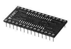
A minor side track: could you use one of these for SOJ devices? I.e. is the spacing the same with the pins as the SOJIC? Forgive my ignorance as I've never dealt with SOJ/SOJIC.
http://uk.mouser.com/ProductDetail/Arie ... mh6pEqc%3d


Top
 Profile  
Reply with quote  
 Post subject: Re: Speed & EEPROMs
PostPosted: Thu Jun 18, 2015 1:06 pm 
Offline
User avatar

Joined: Mon May 25, 2015 2:25 pm
Posts: 642
Location: Gillies, Ontario, Canada
The 10ns SOJ packages are easy to hand solder.
I have done this using 3 different moethods; adapter, ribbon wire to socket, and most recently, dead-bugged to socket.

Here is the part at Digikey...

http://www.digikey.com/product-search/en?pv1291=3385&FV=23c0014&k=cy7c1049&mnonly=0&newproducts=0&ColumnSort=0&page=1&stock=1&quantity=0&ptm=0&fid=0&pageSize=25

Garth also has modules available.

Brad


Top
 Profile  
Reply with quote  
 Post subject: Re: Speed & EEPROMs
PostPosted: Thu Jun 18, 2015 2:03 pm 
Offline
User avatar

Joined: Fri Aug 30, 2002 1:09 am
Posts: 8510
Location: Southern California
banedon wrote:
A minor side track: could you use one of these for SOJ devices? I.e. is the spacing the same with the pins as the SOJIC? Forgive my ignorance as I've never dealt with SOJ/SOJIC.
http://uk.mouser.com/ProductDetail/Arie ... mh6pEqc%3d

The one you linked to has .025" square posts, which are too fat to go into a normal IC socket. Aries and others do however have the appropriate adapters. This is what they look like:
Image
I have a few with different numbers of pins here. The adapter usually costs a lot more than the IC, but it sure makes things easy.

_________________
http://WilsonMinesCo.com/ lots of 6502 resources
The "second front page" is http://wilsonminesco.com/links.html .
What's an additional VIA among friends, anyhow?


Top
 Profile  
Reply with quote  
 Post subject: Re: Speed & EEPROMs
PostPosted: Thu Jun 18, 2015 3:54 pm 
Offline
User avatar

Joined: Sun Sep 08, 2013 10:24 am
Posts: 740
Location: A missile silo somewhere under southern England
Thanks guys.
I've already purchased 4x CY7C109D-10VXI and 3x CY7C199D-10VXI so just need to figure out if I can find adapters that are cheap enough to warrant not soldering them myself.


Top
 Profile  
Reply with quote  
 Post subject: Re: Speed & EEPROMs
PostPosted: Thu Jun 18, 2015 5:28 pm 
Offline
User avatar

Joined: Mon May 25, 2015 2:25 pm
Posts: 642
Location: Gillies, Ontario, Canada
http://www.mikronauts.com/proto/154-2/

Brad


Top
 Profile  
Reply with quote  
 Post subject: Re: Speed & EEPROMs
PostPosted: Thu Jun 18, 2015 6:55 pm 
Offline
User avatar

Joined: Sun Sep 08, 2013 10:24 am
Posts: 740
Location: A missile silo somewhere under southern England
Oneironaut wrote:

Nice find, Brad. Just got to figure out how you order them ;)
There's also these:
http://www.ebay.co.uk/itm/New-10-PCS-SO ... 3a9479cfc5


Top
 Profile  
Reply with quote  
 Post subject: Re: Speed & EEPROMs
PostPosted: Thu Jun 18, 2015 7:16 pm 
Offline
User avatar

Joined: Thu Jun 23, 2011 2:12 am
Posts: 229
Location: Rancho Cucamonga, California
Did you look at Schmartboard.com for SMD-to-DIP converter boards?

===Jac


Top
 Profile  
Reply with quote  
 Post subject: Re: Speed & EEPROMs
PostPosted: Thu Jun 18, 2015 8:10 pm 
Offline
User avatar

Joined: Fri Dec 11, 2009 3:50 pm
Posts: 3367
Location: Ontario, Canada
Here's another mounting method for SOJ (below).

Also I've edited my previous post to include a circuit for two wait-states. Compared with no wait states, this results in roughly quintuple (5 times) the available memory access time. /CS is presumed to go low before the start of phase two, as already discussed.

cheers,
Jeff
Attachment:
double-wait-state generator.gif
double-wait-state generator.gif [ 4.32 KiB | Viewed 2117 times ]
Attachment:
J-lead mounting to WW pins.jpg
J-lead mounting to WW pins.jpg [ 63.3 KiB | Viewed 2117 times ]
Attachment:
J-lead mounting to WW pins btm view.jpg
J-lead mounting to WW pins btm view.jpg [ 70.6 KiB | Viewed 2117 times ]

_________________
In 1988 my 65C02 got six new registers and 44 new full-speed instructions!
https://laughtonelectronics.com/Arcana/ ... mmary.html


Last edited by Dr Jefyll on Thu Jun 18, 2015 8:18 pm, edited 2 times in total.

Top
 Profile  
Reply with quote  
 Post subject: Re: Speed & EEPROMs
PostPosted: Thu Jun 18, 2015 8:11 pm 
Offline
User avatar

Joined: Sun Sep 08, 2013 10:24 am
Posts: 740
Location: A missile silo somewhere under southern England
Looking now :).

Brad, how do you normally keep the IC in place? A dab of hot glue? Blutack? (:D)


Top
 Profile  
Reply with quote  
 Post subject: Re: Speed & EEPROMs
PostPosted: Thu Jun 18, 2015 8:33 pm 
Offline
User avatar

Joined: Sun Sep 08, 2013 10:24 am
Posts: 740
Location: A missile silo somewhere under southern England
Dr Jefyll wrote:
Here's another mounting method for SOJ (below).

Also I've edited my previous post to include a circuit for two wait-states. Compared with no wait states, this results in roughly quintuple (5 times) the available memory access time. /CS is presumed to go low before the start of phase two, as already discussed.

cheers,
Jeff
Attachment:
double-wait-state generator.gif
Attachment:
J-lead mounting to WW pins.jpg
Attachment:
J-lead mounting to WW pins btm view.jpg

Hmmm this is quite interesting. For my next design I'm planning to use bank swapping which has the ability to specify the FROM bank and the TO bank separately when specifying READ and WRITE operations (basically for code copying).
Thus I could set up the following:

$0000-$1FFF - non-swap RAM area for ZP, stack and user/program space (area always stays available)
$2000-$7FFF - swap bank area A (RAM banks A0,A1,A2,A3)
$8000-$AFFF - non-swap I/O area (area always stays available)
$B000-$FFFF - swap bank area B (banks B0, B1)

B0 will be ROM
B1 will be faster RAM

On boot, B0 is selected. It copies boot strap code to page 0
This code runs a copy of bank B0 to B1, swaps to bank B1
Code is then executed from a point in the new 'rom' area in B1

Looks do-able to me.


Top
 Profile  
Reply with quote  
Display posts from previous:  Sort by  
Post new topic Reply to topic  [ 48 posts ]  Go to page 1, 2, 3, 4  Next

All times are UTC


Who is online

Users browsing this forum: No registered users and 43 guests


You cannot post new topics in this forum
You cannot reply to topics in this forum
You cannot edit your posts in this forum
You cannot delete your posts in this forum
You cannot post attachments in this forum

Search for:
Jump to: