MOS 6509 look-alikes?

For discussing the 65xx hardware itself or electronics projects.
User avatar
Dr Jefyll
Posts: 3526
Joined: 11 Dec 2009
Location: Ontario, Canada
Contact:

Post by Dr Jefyll »

sjgray wrote:
Each bank [...] has it's own zero page and stack.

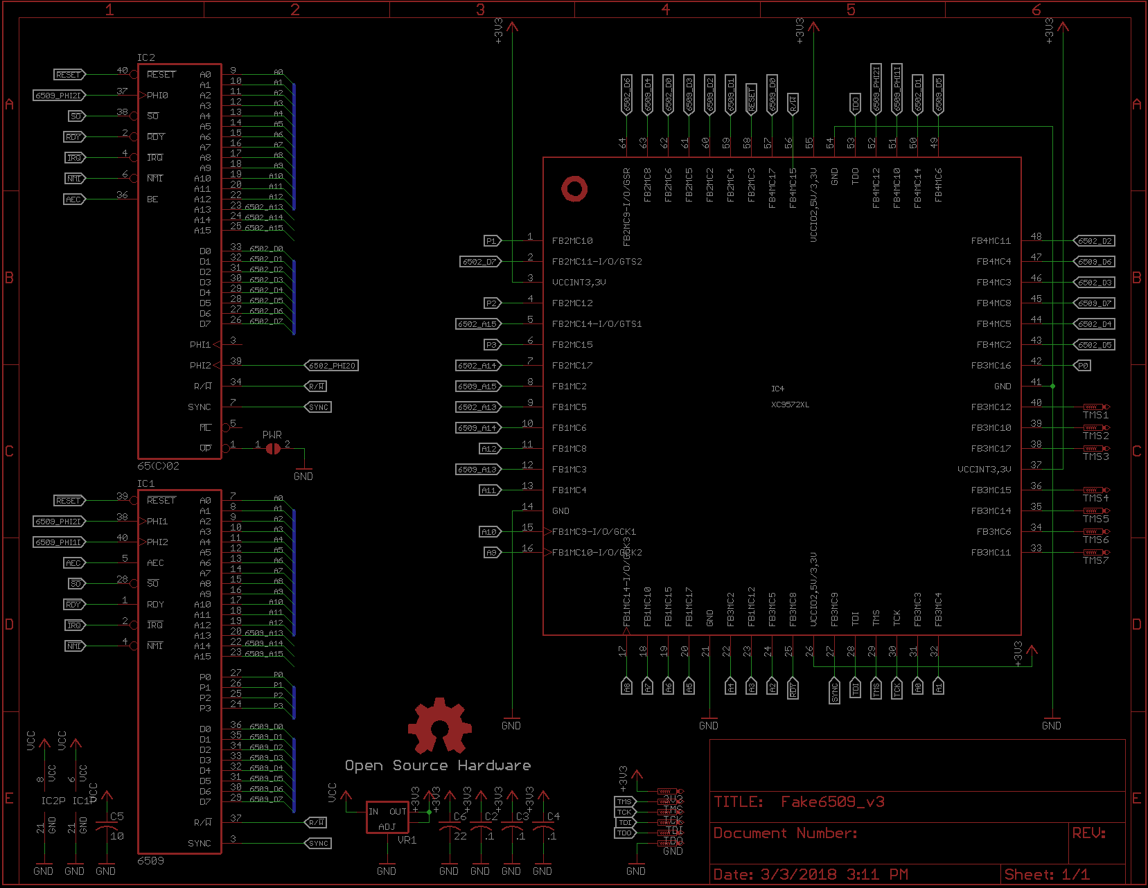
Thanks, Steve. I think this reveals the 6509 is not a specially designed CPU -- instead it's just a sidecar hung on the 6502 (sort of like the 2A03, which uses a stock 6502 mask but with a bit of extra logic added around the perimeter). Here is my version of add-on logic for a 6509 look-alike. If my understanding of the 6509 is correct, then this circuit, connected to a 6502, should reproduce 6509 behavior. [Edit: confirmed -- see subsequent posts.]
6509_look-alike.png
6509_look-alike.png (11.21 KiB) Viewed 10190 times
I drew this with 6502 in mind but offhand see no reason it wouldn't be OK for the 'C02 or even the '816. The circuit detects the opcode fetch of the two modified 6509 instructions, STA (Ind),Y and LDA (Ind),Y (op-codes $91 and $B1). The data access occurs later -- either during in cycle 5 or 6. It'll be cycle 5 only if the access is a read and no page crossing occurs, as per normal 6502 behavior. During cycle 5 (and cycle 6, if it's present) the Indirect memory bank is selected by the 74_157 mux. If it's a read with no page crossing, cycle 6 will be absent, as per normal 6502 behavior. In that case the circuit uses SYNC to ensure it'll be the Execution bank that's selected for the opcode fetch in the cycle which follows cycle 5.
Note:
  • I haven't bothered to draw the output port logic that provides the two bank addresses.
  • the '377 is an octal, edge-triggered register similar to '374 or '574, but clocking with /EN high ignores the new input data on D and reloads the data already on Q. IE: the output remains unchanged.
  • The XOR gate protects against the false opcode fetch that occurs whenever an interrupt is recognized. There's a risk that a $91 or $B1 opcode will get fetched but not executed. If this happens the circuit mustn't respond. To recognize the beginning of the cpu's interrupt sequence we look for the unique circumstance of the address bus failing to increment in the cycle following an opcode fetch. No increment means the least-significant address line, A0, will fail to toggle. The output of the XOR gate will be low, thus inhibiting the circuit.
  • To simplify the circuit D1 could be ignored (like D5). This would render the circuit susceptible to triggering from opcodes $93 and $B3, but these are undefined op's anyway.
mdpenny wrote:
"hacking" an '02 with external logic would likely impose limits on performance
Right, Martin -- certainly that's a legitimate concern for this circuit (in its present form). For example in some situations there'll be no valid bank address until SYNC has had time to propagate into the mux. At NMOS CPU speeds that's a fairly trivial delay, but for a modern 'C02 running at, say, 14 MHz, it's much more of an issue. Hmmm.... For the '816 you could make use of VPA and VDA signals, which would inform you in cycle 5 whether there's a page crossing. Having that advance notice means you could use fully synchronous logic and eliminate the performance limit. IOW you could 6509-ify an '816 and run it at the full 14 Mhz.

The FPGA approach is attractive too, of course. (I mean with the cpu core implemented on FPGA.) The add-on approach could be abandoned for something more elegant and resource-efficient!

Since the goal seems to be to run pre-existing CBM-II code, the question arises whether the FPGA core would have to accurately reproduce undefined 6502 op's. Do CBM-II applications use illegal instructions?! (This issue would also affect the 'C02 and '816 add-on look-alikes.)

-- Jeff

Edits: Fix typo. Improve clarity. Fix booboo: '377 register, not '273.
Edit (2018): Improve clarity. Fix booboo: the Enable on a '377 is active low, not active high. The updated diagram reflects this. Also, the original logic (shown below) unnecessarily imposed two gate delays between SYNC and the mux.
previous version of logic.png
previous version of logic.png (1.93 KiB) Viewed 10190 times
Last edited by Dr Jefyll on Fri Dec 28, 2018 2:33 am, edited 5 times in total.
User avatar
BigEd
Posts: 11464
Joined: 11 Dec 2008
Location: England
Contact:

Post by BigEd »

Excellent! About the speed concern: wrapping all this glue, including the two ports, into a CPLD, is a possible answer. I haven't counted up the required pins though. An off the shelf CPU plus a CPLD is a useful step, short of going for a custom CPU on an FPGA. And for this level of complexity it's natural to design with schematics, so no particular need to learn an HDL.

That said, the same design could readily be combined with an existing 6502 core in an FPGA.

Cheers
Ed
fachat
Posts: 1124
Joined: 05 Jul 2005
Location: near Heidelberg, Germany
Contact:

Post by fachat »

Excellent work indeed!
Dr Jefyll wrote:
Note:
  • ...
  • The XOR gate protects against the false opcode fetch that occurs whenever an interrupt is recognized. There's a risk that a $91 or $B1 opcode will get fetched but not executed. If this happens the circuit mustn't respond. To recognize the beginning of the cpu's interrupt sequence we look for the unique circumstance of the address bus failing to increment in the cycle following an opcode fetch. No increment means the least-significant address line, A0, will fail to toggle. The output of the XOR gate will be low, thus inhibiting the circuit.
  • ...
That was my initial concern but you have handled that as well! Great work! Only one question: Have you run that through visual 6502 that there is a cycle where PC is not incremented before the IRQ handling starts? Otherwise assume the opcode is on an odd address, the IRQ kicks in, and then what happens in the two "internal operations" cycle, maybe it does actually increase PC? I couldn't find this on a quick search...

André
User avatar
Dr Jefyll
Posts: 3526
Joined: 11 Dec 2009
Location: Ontario, Canada
Contact:

Post by Dr Jefyll »

Right, then! If that goofy kludge makes sense to you guys then I know I'm not completely crazy! (Or, if I am, at least I have some company.)
BigEd wrote:
There's no need to limit to 4 bits of bank address either
Quite right. Our add-on logic needn't be limited to 1 MB (4 extra address bits). We can easily go as high as 16MB (8 extra bits) -- or even higher if we find a way to map in wider ports.

Actually I'm disappointed to learn that the 6509 is so primitive. On the one hand it is better than conventional mapping schemes that deal in, say, 8K or 16K chunks. (These clever but constricting schemes seem to be by far the most widely adopted means of beating the 64K barrier.)

On the other hand, the 6509 falls short of what it could have been. Because it maps the ports to $0000 and $0001 of every bank, the 6509 is incapable of hosting an array or other object greater than 64K-2 in size. IMO this limits you to small-computer goals, in contrast to the '816 and and my Kimklone which let you accommodate and linearly address any object that'll fit in memory.
fachat wrote:
I couldn't find this on a quick search...
The lack of PC incrementing during interrupt recognition is documented on page A-11, Table A. 5.4 of the MOS Hardware Manual and in Table 5-7 of the '816 Data Sheet. There's an old and somewhat fragmented 6502.org discussion of the topic here. See also the visual6502.org/wiki/ page here.

cheers,

Jeff
[edited to include Ed's comment and the link to the visual6502.org wiki page]
sjgray
Posts: 29
Joined: 15 Aug 2009

Post by sjgray »

Nice! 6509's are in very short supply... Anyone willing to build and test?!

Steve
User avatar
Dr Jefyll
Posts: 3526
Joined: 11 Dec 2009
Location: Ontario, Canada
Contact:

Post by Dr Jefyll »

I wrote:
Do CBM-II applications use illegal instructions?!
Still curious about this point. If we don't need to preserve the illegal op's then the '816 may be better than an '02 in regard to creating a 6509 substitute using add-on logic.

Steve, is your Rogers email working properly? I haven't heard back from a msg I sent you on Friday. Maybe you're just enjoying the holiday...

Jeff
sjgray
Posts: 29
Joined: 15 Aug 2009

Post by sjgray »

Dr Jefyll wrote:
I wrote:
Do CBM-II applications use illegal instructions?!
Still curious about this point. If we don't need to preserve the illegal op's then the '816 may be better than an '02 in regard to creating a 6509 substitute using add-on logic.

Steve, is your Rogers email working properly? I haven't heard back from a msg I sent you on Friday. Maybe you're just enjoying the holiday...

Jeff
Holidays have been crazy... Sorry, I seemed to have missed your email.
Things have settled down now, thankfully.

Btw, I'd be surprised if any cbmii software used illegal opcodes, simply because there's so little software for the machines.

Steve
brain
Posts: 113
Joined: 05 May 2009

Re: MOS 6509 look-alikes?

Post by brain »

Sorry for resurrecting a long ago thread, but I created a PCB for a 6509 Replacement:

Image
Image

I am considering building a few test boards, if someone is interested in testing.

Jim
User avatar
BigDumbDinosaur
Posts: 9427
Joined: 28 May 2009
Location: Midwestern USA (JB Pritzker’s dystopia)
Contact:

Re: MOS 6509 look-alikes?

Post by BigDumbDinosaur »

brain wrote:
Sorry for resurrecting a long ago thread, but I created a PCB for a 6509 Replacement:
...
I am considering building a few test boards, if someone is interested in testing.

Jim
I can't read what is in your images.
x86?  We ain't got no x86.  We don't NEED no stinking x86!
User avatar
BigEd
Posts: 11464
Joined: 11 Dec 2008
Location: England
Contact:

Re: MOS 6509 look-alikes?

Post by BigEd »

Thanks Jim, that's a very interesting development!
sjgray
Posts: 29
Joined: 15 Aug 2009

Re: MOS 6509 look-alikes?

Post by sjgray »

Very nice! This is long overdue.

Steve
DerTrueForce
Posts: 483
Joined: 04 Jun 2016
Location: Australia

Re: MOS 6509 look-alikes?

Post by DerTrueForce »

It's usually a good idea to post schematics in black and white, because there are some people here that are colour-blind.
User avatar
BigEd
Posts: 11464
Joined: 11 Dec 2008
Location: England
Contact:

Re: MOS 6509 look-alikes?

Post by BigEd »

For reference and for interest, there's a long and active thread over on the cbm-hackers mailing list discussing "Hardware emulation of 6509 using 6502?" which are worth a read - hopefully as and when some excellent discoveries are made or conclusions reached we can summarise or link to them:
http://www.softwolves.com/arkiv/cbm-hac ... html#25459
http://www.softwolves.com/arkiv/cbm-hac ... html#26201
brain
Posts: 113
Joined: 05 May 2009

Re: MOS 6509 look-alikes?

Post by brain »

BigEd wrote:
For reference and for interest, there's a long and active thread over on the cbm-hackers mailing list discussing "Hardware emulation of 6509 using 6502?" which are worth a read - hopefully as and when some excellent discoveries are made or conclusions reached we can summarise or link to them:
http://www.softwolves.com/arkiv/cbm-hac ... html#25459
http://www.softwolves.com/arkiv/cbm-hac ... html#26201
It's a shame the Interwebs have not found a way to "join" a discussion across two forums, as the cbm-hackers thread is a direct continuation of this thread.

In short:

I implemented Dr. Jefyll's schematic from this thread in a small piggyback PCB.
We determined that the design also should trap the databus, so as to not read from the computer during a $0/$1 read (next design rev)
There are potential issues with the CLK signal (6509 uses external clocks, 6502 creates them internally)
Currently, we are tracking down a problem where a write on the 6502 does not push the right value to the databus (or, it does not keep it there long enough)

There's a companion thread to discover the specific nature of the indirect addressing (page crossings, behavior when writing value, etc.)

Jim
User avatar
BigEd
Posts: 11464
Joined: 11 Dec 2008
Location: England
Contact:

Re: MOS 6509 look-alikes?

Post by BigEd »

All very interesting Jim, thanks for the update!
Post Reply