Joined: Thu May 28, 2009 9:46 pm
Posts: 8514
Location: Midwestern USA
|
So, I’ve been monkeying with POC V2.0, still with the NOP ROM, so I could further study the bus timing during a data fetch to see how good (or bad) my design seems to be. Executing NOPs is good for this purpose, since the instruction consists of the opcode fetch cycle and a “dead” cycle. The 65C816’s behavior during the dead cycle is kind of interesting, but that’s a topic for another post.
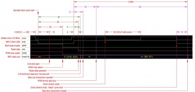
Anyhow, I generated a new annotated logic analyzer capture for your viewing pleasure:
Attachment:
 read_timing_annotated_reduced.jpg [ 425.92 KiB | Viewed 899 times ]
In the above, the notations above the capture are times in nanoseconds. These times need to be taken with a grain of salt, as the logic analyzer’s maximum resolution is 2ns (500 MHz sampling clock). So right off the bat, the clock period isn't necessarily what it appears to be.
Ø2 is 16 MHz when not being stretched during a wait-state, which produces a 62.5ns clock period, or a 31.25ns half cycle. The logic analyzer has to fudge with displaying these signals, which creates some minor oddities with, for example, GCLK (global clock, which is the time base for the entire mess) and Ø2. In actuality, these signals are always in phase, except during a wait-state. Because of the logic analyzer's rounding to the nearest 2ns, it appears the two clocks are 2ns out of phase during the opcode fetch cycle. This artifact is gone by the time Ø2 falls at the end of opcode fetch—apparently the logic analyzer did some more fudging at that point.
The data bus is being sampled by the logic analyzer on the inward (MPU) side of the bus transceiver. The presence of the transceiver has some interesting effects. The transceiver is closed during Ø2 low to prevent any possibility of bus contention. The bank bits persist for 6ns after the rise of Ø2. However, /RD (read data) goes low 4ns after the rise of Ø2. It is at this point in the cycle where the MPU could theoretically get into a shoving match with whatever device has been selected. However, the transceiver doesn't open for business until 8ns after the rise of Ø2. By then, the MPU has turned around the data bus and the window of opportunity for contention has been closed.
Note that the ROM doesn't start emitting data until some 20ns after the rise of Ø2—this is a 45ns ROM. The ROM's /CS (chip select) is being asserted 10ns before the rise of Ø2, so the ROM is performing substantially better than specified. Also notice /WSE (wait-state enable) is apparently simultaneously asserted with /CS. This is likely for real, since buried logic is used to trigger chip selects and /WSE, if ROM or I/O is selected. As the buried logic is combinatorial, it has a vanishingly-small amount prop time. That would explain why /CS and /WSE appear to be simultaneously asserted.
The $FF data bus pattern seen at the point where the transceiver is opened is being generated by pullup resistors that are on the outward (device) side of the transceiver. The resistors help TTL devices push the data lines closer to CMOS territory, as well as prevent the bus from floating whilst the transceiver is closed, since the transceiver will high-Z its signal pins at that time. The $FF pattern persists until the ROM produces some output. This is of no concern to the MPU, since it doesn't sample the data bus until just before the fall of Ø2.
Once the opcode fetch cycle has completed, the MPU will execute a dead cycle. I didn't show the details of that, but some shenanigans involving addressing do occur. Even though it’s a dead cycle and the MPU doesn't perform any external operations, it does emit A16-A23 during Ø2 low. VDA || VPA is false during that time, and since those signals are accounted for in the glue logic, the ROM’s /CS is deasserted during the dead cycle. Also, very shortly after the fall of Ø2, the transceiver will close, which occurs well before the MPU starts emitting A16-A23 again. I show that as occurring at 10ns, but again, the logic analyzer has to fudge and hence there is some uncertainty involving the fall of Ø2 and the response time of the transceiver. As I am using a 74ACT245 transceiver, the maximum specified for that time is 11ns on 5 volts. The transceiver in POC V2.0 appears to be a little faster than that, but it’s not a critical situation.
One other thing mentioned in an earlier post, but worth noting again, is the window of opportunity to cleanly trigger a wait-state is relatively small—it has to occur before the rise of GCLK. I'm cutting it somewhat close in this design, which is, as I also earlier noted, why the maximum reliable Ø2 rate is 16 MHz. Other than that, it appears my logic timing is acceptable and the bodge wire is safe...for now. 
_________________ x86? We ain't got no x86. We don't NEED no stinking x86!
|
|


