6502.org Forum  Projects  Code  Documents  Tools  Forum
It is currently Sun Nov 24, 2024 7:23 am

All times are UTC


Post new topic Reply to topic  [ 7 posts ] 
Author Message
PostPosted: Sun Nov 07, 2021 4:41 pm 
Offline
User avatar

Joined: Sun Nov 07, 2021 4:11 pm
Posts: 101
Location: Toronto, Canada
Hello! This is my first post, although I've been reading and learning from the forum for a few months now. I recently took the plunge into building a 65c02 computer, but I should say that I am an absolute beginner at any kind of hardware design. I've played a bit with Arduino in the past, but otherwise my background is in software, and I'm still trying to really understand some of the basics.

In my board, I have an MCU (an ESP32) that performs some I/O tasks, one of which is interfacing with a PS/2 keyboard. The MCU runs at 3.3V, while the PS/2 interface runs at 5V, and so I've had to add a level shifter in between the two. Originally, I just had a couple MOSFETs (one for the clock line, and the other for data) with a 10k pull-up resistor on both sides.

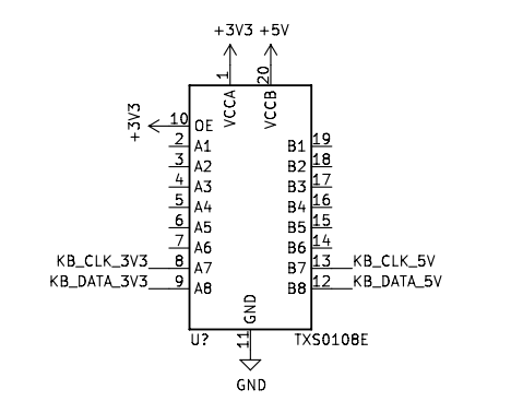
This worked well, but it took up a bunch of space on my board, so I decided to try my hand at a proper bidirectional level shifter, and landed on the TXS0108E (which seemed to be like a good fit, particularly given that, at some point, I also want the MCU to talk to the 65C02 side of the circuit, which also runs at 5V). My circuit looks a little like this:
Image

(Note that the TXS is on a breakout that also includes decoupling capacitors.) I don't have any pull-up resistors here, because my understanding is that the TXS has them built in—and, indeed, the lines are high on both sides when there is no activity.

Now to my problem: for some reason that I do not understand, the signal on both lines looks like this:

Image

This is the data line, as the keyboard is trying to send data to the host. You can kinda see the transmission happen, but it's dirty and causes all kinds of spurious readings at the keyboard end. If you zoom in to the solid-yellow areas, they turn out to be some kind of very tight sine wave at ~2x the clock speed of the keyboard.

This only seems to happen if the keyboard is connected to the TXS breakout board. As far as I can tell, is happens regardless of whether the MCU is connected at the other end. (FWIW, the MCU's pins connected to the lines are both set to inputs.)

This is what I've tried so far:

- I've validated that the signal coming out of the keyboard is clean (-ish… there is a bit of ringing, but it doesn't look like what's showing up in the scope).
- I think that all the connections are OK—I originally wired this on a breadboard, but then soldered it on a protoboard, just in case.
- The TXS seems to work as I would expect; if I manually pull the lines high and low, I see the correct change on the other side. Speed shouldn't be an issue here, as the PS/2 protocol is in the teens of KHz.
- I've googled the TXS and found a bunch of folks having trouble with it, but their problem seems to have been not tying OE to +3V, which I don't think is my problem.

Obviously, I can go back to my MOSFETs (or even just use a voltage divider), but now I feel like I'm missing something very foundational, and so I would love to take this as an opportunity to learn something new. I'm kinda hoping that someone with more experience will immediately see what's wrong :-)

Thanks in advance for all your help!


- TXS0108E datasheet in case someone needs to read it.
- The breakout board I'm using. Given that it came from China and was suspiciously inexpensive, I've already swapped a few different ones in, so I really hope that's not the problem!


Attachments:
DS1Z_QuickPrint1.png
DS1Z_QuickPrint1.png [ 43.21 KiB | Viewed 532 times ]
Screen Shot 2021-11-07 at 11.21.25 AM.png
Screen Shot 2021-11-07 at 11.21.25 AM.png [ 30.66 KiB | Viewed 532 times ]
Top
 Profile  
Reply with quote  
PostPosted: Sun Nov 07, 2021 10:58 pm 
Offline

Joined: Fri Apr 15, 2016 1:03 am
Posts: 140
That's an interesting part!

Try tying the unused A pins to VccA & unused B pins to VccB.

Use your 'scope to measure each of the IC pins. Are Gnd & VccA & VccB present & clean?


Top
 Profile  
Reply with quote  
PostPosted: Mon Nov 08, 2021 2:48 am 
Offline
User avatar

Joined: Sun Nov 07, 2021 4:11 pm
Posts: 101
Location: Toronto, Canada
leepivonka wrote:
Try tying the unused A pins to VccA & unused B pins to VccB.

Use your 'scope to measure each of the IC pins. Are Gnd & VccA & VccB present & clean?


Thanks—I think you may actually be on to something. I did check the voltages at the chip itself (with some difficulty… the thing is tiny!) and everything looked okay.

However, now I have one of these breakout boards providing an actual interface between the ESP32 and the rest of the board with the 6502 bus running at 5V, and everything works as advertised (including a PWM signal running at 10MHz). The only two differences from the keyboard setup is that all the I/O lines are used, and that this interface is push-pull instead of open-collector. So, unless there's some specific exception that applies to open-collector circuits, I think that you may be right, and without all pins connected to something, the chip is up to no good.

Unfortunately, I broke my only good PS/2 connector, so I'll have to wait until I get a new one before testing. I'll report back—thanks again for the suggestion!


Top
 Profile  
Reply with quote  
PostPosted: Mon Nov 08, 2021 7:22 pm 
Offline
User avatar

Joined: Fri Dec 11, 2009 3:50 pm
Posts: 3367
Location: Ontario, Canada
CountChocula wrote:
Originally, I just had a couple MOSFETs (one for the clock line, and the other for data) with a 10k pull-up resistor on both sides.
Can you share the original circuit with us, please?

I seem to recall that the usual interface for that type of keyboard uses Open Collector drivers to pull the lines low, and that the lines go high only due to the action of pullup resistors. (It's a simple arrangement, and one that allows the lines to be alternately driven from the keyboard end and from the host computer end... and yet, no tri-state buffers are required.)

I suspect the TXS0108E is not an appropriate replacement for an Open Collector driver in this use case. An Open Collector driver can pull low but, by design, it has no ability to pull up. (You were probably using the MOSFETs in the same way. :wink: ) I'm half guessing, but maybe the TXS0108E is pulling up at times, and that's what's causing your difficulty.

If you want a space saving alternative to a MOSFET, you can consider using one of the tiny gates in the 1G and 2G series. There are numerous offerings, including a few Open Collector (actually Open Drain) devices. See my post, Tiny, superfast gates rival programmable logic.

Note that a 74LVC2G06 dual open-drain inverting buffer will replace two MOSFETs.

I'm attaching a photo of three 1G Series devices located on a breakout board. These are SOT-23 packages, but even smaller options are available. The SOT-23 is plenty small enough for me! :shock: :lol:

-- Jeff


Attachments:
IMG_2756CrpTchLores.JPG
IMG_2756CrpTchLores.JPG [ 82.4 KiB | Viewed 430 times ]

_________________
In 1988 my 65C02 got six new registers and 44 new full-speed instructions!
https://laughtonelectronics.com/Arcana/ ... mmary.html
Top
 Profile  
Reply with quote  
PostPosted: Mon Nov 08, 2021 9:32 pm 
Offline
User avatar

Joined: Sun Nov 07, 2021 4:11 pm
Posts: 101
Location: Toronto, Canada
Well, I couldn't wait for the new parts to arrive, so I jury rigged the PS/2 port with—I kid you not—a couple paperclips, and connected all the unused lines to VCCa/b as leepivonka suggested, and lo and behold:

Image

So, it seems that that was the problem. Thank you so much for your suggestion! Now for a follow-up: Is this the kind of thing that one is just “supposed to know” based on experience, or is it explained somewhere on the datasheet? I find these documents hard to read, probably because they assume the level of knowledge that makes sense for an EE, but not for someone like me who is just starting out.

@Dr Jefyll: I have deleted that, but it was more or less similar to this one. My understanding of the PS/2 protocol (from what I have read, e.g. here) is that the lines are held high unless pulled low by either the host or the device… so, if I'm reading the datasheet correctly, the TXS should be able to do the job (and indeed, it looks like it can… I had just wired it wrong).

Those gates you posted are super cool, though… I'm going to order some and play with them. Thanks for the suggestion!


Attachments:
DS1Z_QuickPrint2.png
DS1Z_QuickPrint2.png [ 39.74 KiB | Viewed 411 times ]
Top
 Profile  
Reply with quote  
PostPosted: Mon Nov 08, 2021 9:50 pm 
Offline
User avatar

Joined: Thu Dec 11, 2008 1:28 pm
Posts: 10986
Location: England
Datasheets are usually very handy, and will reward a close and careful reading.

But it is a fairly regular thing that unconnected inputs on chips will cause trouble - it's maybe slightly unexpected in this case, as the inputs are not regular inputs, but it's consistent really, to tie them off.


Top
 Profile  
Reply with quote  
PostPosted: Tue Nov 09, 2021 12:58 am 
Offline
User avatar

Joined: Sun Nov 07, 2021 4:11 pm
Posts: 101
Location: Toronto, Canada
Fair enough—I'll file it away as one more lesson learned then :-)

Cheers!


Top
 Profile  
Reply with quote  
Display posts from previous:  Sort by  
Post new topic Reply to topic  [ 7 posts ] 

All times are UTC


Who is online

Users browsing this forum: No registered users and 56 guests


You cannot post new topics in this forum
You cannot reply to topics in this forum
You cannot edit your posts in this forum
You cannot delete your posts in this forum
You cannot post attachments in this forum

Search for:
Jump to: