Controller: (input decoding stuff)Proxy wrote:
i mean a VIA would make connecting some buttons pretty easy

I am greatly tempted to add a VIA. more later.
Quote:
but since you want to use discrete logic, you can do it like the NES. which only latches the controller inputs when the CPU wants to read them. though the NES controller used a shift register because it send the data over a serial line. in your case all buttons are directly on the PCB so you could get away without a latch and just use a simple tri-state buffer (and maybe some debouncing circuitry). the buffer would be enabled whenever the CPU reads from a specific address, which depends on how your logic is built.
Yes, in fact not going through the serial line that makes things slightly different, because of this certain chips just wont work, even though they have a reset/clear function and 8x tristate outputs...
Just using a simple Latch/Buffer is probably ok., yet it has its own challenges. I have a choice of several chips. the 74573 is pretty simple as a 'gate', its just a single pin and the 'data side' goes to the 6502.. I think this might be easy to wire up maybe...
Ultimately, yes, just like an NES controller, this device has only 8 input buttons, mapped to a specific address in RAM, one bit for each button, up.down.left.right.red.blue.yellow.green. I will discuss use of a VIA below.
cjs wrote:
wayfarer wrote:
what I am after is when a button is pressed, it latches to an input. polled by the CPU every so often and clears the buffer. ...
This is roughly the way keyboard scanning works on many '70s and '80s 8...
gotcha, I am not putting a full keyboard on here, it will be an onscreen menu, like a game or industrial machine. Just 8 buttons as mentioned. This is to keep it simple and minimize complexity and hardware connections. one of my next builds will have a calculator keypad and additional buttons.
Quote:
It will probably easier not to have the buttons latch when they are pressed but instead just let their state be their state, whatever it is when you scan them. (... None of the systems I've examined do any debouncing at all, so it seems that as long as you're scanning the buttons frequently enough, but not too frequently, everything there is fine. ...
So the trouble here is 'missing' an input because of operator timing, when you are playing a game, and you push a button, you should not push it several times and hope it connected; so I am thinking a latch and some software says if held down or hit repeatedly. There is a buffer and it actually looks simple and not too bad, its in the picture below, the 74'573. It just needs two control pins, more on that below. It would just 'expose the pins' when told to, so addressing on that just needs to turn everything off and let it be on the data buss... not too bad I think
Quote:
If you want to study some hardware and code that uses this technique, ...
On a future project yes, this is such a deep dive for this, its
beyond the scope of an altoids can.
cjs wrote:
i'd recommend putting all your IO in roughly the same area, for example 256 bytes directly at the start of your ROM (let's say $C000-$C0FF). that would mean your decoding logic checks if the upper 8 bits of the address bus are equal to $C0, and if true generate a single "IO Enable" signal which you can use with the lower 8 bits of the address bus to see which IO decide specifically is being addressed. that way you decode IO Addresses in 2 steps, with the upper 8 bits taken care of by a single comparator, so you only need to worry about the bottom 8 bits per IO device, which makes the logic a bit easier if you have multiple IO devices. (at the expense of some propagation delay)
at least that's how i do it on my SBCs!
I only have a few devices, keypad and screen... I might sack a byte to output to a sound chip... again, a VIA here is attractive. I am moving to an 8k EEPROM, it frees up control lines and simplifies things, I would be placing I/O just below that or just above RAM.
Quote:
On a side note, with RAM it doesn't matter how you order the address or data lines when connecting to the CPU, it will still work perfectly fine. so for those you can map the lines however it fits best with your routing.
[/quote]
so here it seems I can or should do that, though exactly how was not lining up as expected. the design below is much cleaner.
Address Decoding: latches and buffers and gates oh my!
Quote:
Quote:
so, if I have an 8-bit latch tied to a set of 8 buttons, how do i make that byte... $FFF1-FFF2 or whatever that is available to the CPU to read?
And there's the rub: now you're into dealing with address decoding. I mentioned this earlier, but I suspect you didn't fully understand it, or at least its implications. In your current schematic I note that the chip selects for your RAM, ROM and display are all unconnected; you need to have an address decoding system that deals with all of these, too, as well as your button interface.
yes this is the part I am trying to sort out. The 6502 doesn't have any Chip Select lines.
Quote:
I would start with
Address Decoding from the Wilson Mines 6502 primer. Once you've digested that, I cannot strongly enough recommend examining and understanding the address decoding on some existing systems such as
Grant's 7-chip 6502 computer, ...perhaps including a commercial computer or two ...
I did look several of these over and you almost see an idiomatic way of connecting things. The schematic below has more of this done correctly.
Quote:
I suspect the simplest system will be to reduce your ROM to 16K and have your display at $8000-$9FFF and buttons at $A000-$BFFF. (Or if you need more ROM and less RAM, reduce RAM to 16K and put your display at $4000-$5FFF and buttons at $6000-$7FFF.) Design this out to get a sense of how it works. If you want to get much more complex than that, you'll probably start to see why people like to use PLAs, CPLDs or microcontrollers emulating devices for this sort of thing.
so I am going with 32K RAM from 0000-7FFF, 8K ROM to upper block E000 (for EEPROM, lolz) through FFFF, this will maintain all vectors. This leaves "8K" open to use for I/O and any screen mapping, about 8K. I could just about leave the controller inputs, at 0000 or whatever, as it will just 'be on the data lines' if I send I bit to it on the 74573, its just an 'enable pin', the other pin Id probably just wire static.
So, I have looked at several schemes:
http://wilsonminesco.com/6502primer/potpourri.htmlhttps://eater.net/schematics/6502.pnghttps://preview.redd.it/olj13ery7f841.j ... 03c67ae822https://preview.redd.it/levfg7dz9f841.j ... 49f3efdca4https://preview.redd.it/lrfnm9259f841.j ... 2259307b70there seems to be an idiomatic way of doing things, I can probably get away with not using a VIA, though it has a LOT going for it.
If my RAM does not use A15, then I want it's CS or Enable to be inverted from this one pin, this is the fastest way to start Chip Select, as with 1 bit, upper and low address space is on or off, so, A15 is a 'Primary' control line.
When A15 is on (need to get more used to and familiar with high or low), then 'all the other stuff is on' and RAM is 'off'.
Next is ROM, and uses A0-11 (12 bit, 8k) and does not use A14 or A13, so there are two other control lines. I wont need a Write Enable on the ROM for this, it will be held 'off/no write'. so ROM needs few lines. Next is display and it needs a couple of control lines and the data buss for commands and data with 8k internal RAM you can read from, though I have no intention to. it will mostly just be a single address you send to over and over again, it doesnt map its RAM to the address buss, it just serves whatever you request several cycles later back to the data buss. and then the buttons just go 'wherever' because its only going to be a gate with an Output Enable bit to expose it to the Data buss.
So, that would map fairly idiomatically to a 7400 NAND arrangement.
A15 is CS RAM/Other
A14/A13/A12 is free if A15 is on.
A14 = ROM
A13 = Display
A12 = Buttons
I very much think there is a way here to use an inverting transistor (which can take the place of a wire in this cramped space with its leads) instead of a full NAND... if there were a way to use the 6502 pins as a CS line... or such, basically any other control line of some type, OE, CS, etc...
I didnt see one though.
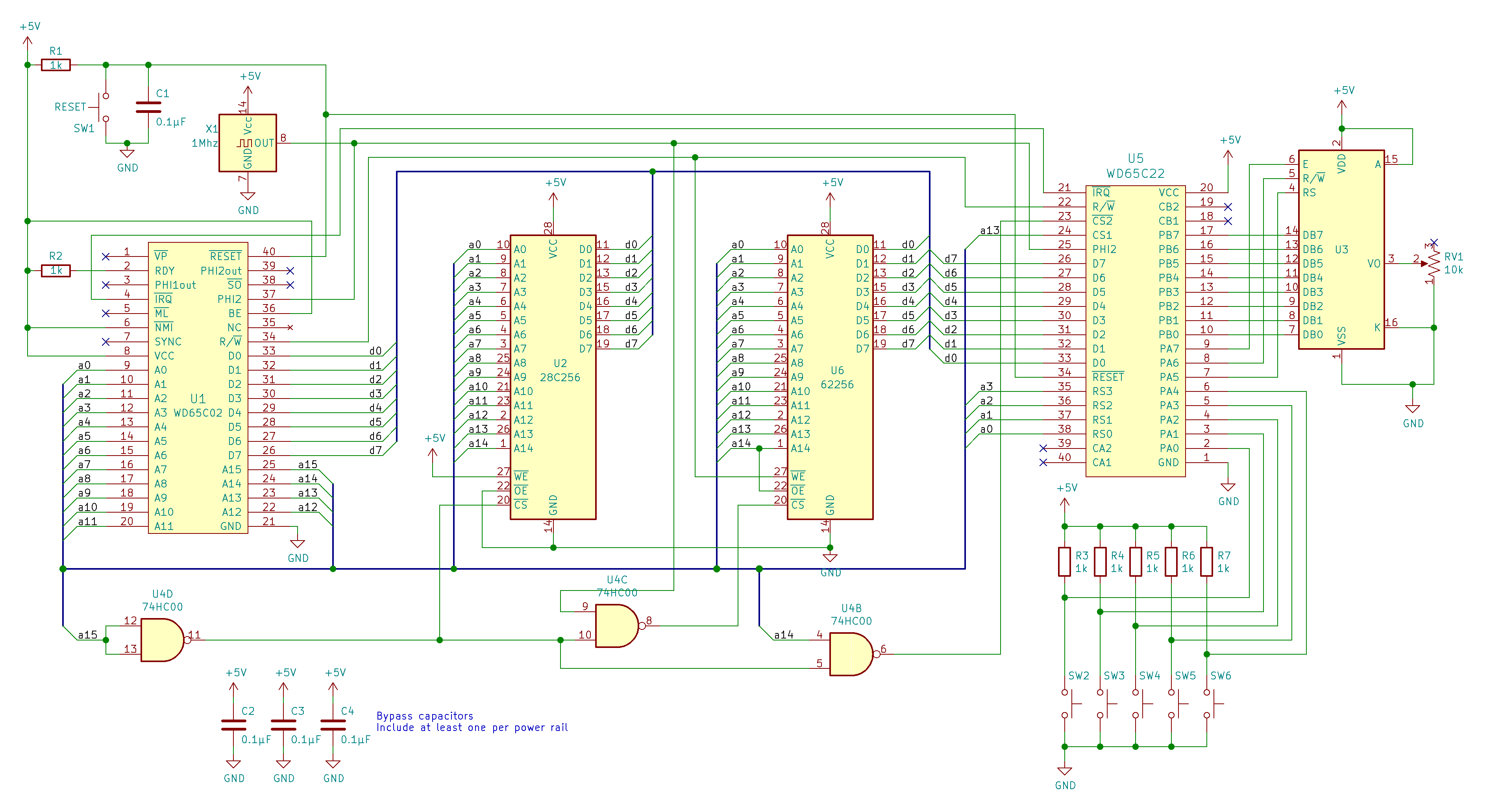
I am highly interested in adding a 6522, it complicates and simplifies things. It seems like any Address Pins lost to it are recovered with CA1/2 and CB1/2, plus the Ports, and the internal registers and functions. If I can run without it I will, though I wonder if I can use a 6522 without a 7400... if so, the 74573 is 20 pins and a 7400 NAND is 14 and so totally justified. On future designs (I found a nice standard enclosure on mouser/digi for about $10) I will use on future builds) having a GPU, a VIA and a USB or DB-9 will be standard, probably an SD card or similar.
for now though, its just a mint can and a 6522 is cool yet extra right now. I ordered one, Ill see if it fits, between a sound chip, the 74573 gate, and any other logic, its a good thing. I could put the display on Port A and the controls and sound and I/O and timers and such on Port B. I almost think it will work. Once you print a board, its no problem, with this perfboard, I dont want it if I can help it. a noise diode turned on and off makes drum sounds...
gotta think like that..
okay, so I think I can get some control lines, I can tie a lot of pins high or low, and it seems RAM is tied to the clock a lot, this is for WRITE operations?
the RAM leaves pin 15 open, when its on, ROM doesnt use 14 or 13, and if the display isnt using those, then pin 12 can OE the 74573 to put the 8 buttons on the data bus to whatever register (Acc)
this does need a 7400 or some other setup then. if I could use the SO, SYNC, BE or MLB pins, I think that might simplify a few things, though they do not seem to be very useful as is.
anyway, I see why the 7400 is so idiomatic, and get the gist of how to set this up. and still not need a 6522 yet, even though it might be a good idea.
if the 6522 could automate block transfers to the display, or otherwise 'do much without needing as much work without it' Id use it for sure.
Attachment:
 image31523.png [ 79.07 KiB | Viewed 942 times ]
I could get a 6522, and replace the 74573 with an audio chip, usb or support circuity maybe... lotta wires though in a can... idk, Ill see if it fits. be cool if it does, would run the display with CA1/CA2 to the video chip selects I guess... so much extra wires, so easy on a PCB with PLCC sockets, lol
Attachment:
 Inkedimage.jpg [ 140.88 KiB | Viewed 939 times ]


