6502.org Forum  Projects  Code  Documents  Tools  Forum
It is currently Wed May 22, 2024 5:40 pm

All times are UTC


Post new topic Reply to topic  [ 22 posts ]  Go to page 1, 2  Next
Author Message
PostPosted: Wed Jun 24, 2015 12:52 pm 
Offline
User avatar

Joined: Tue Feb 10, 2015 5:27 pm
Posts: 80
Location: Germany
Hi,


I wonder if someone knows why MOS designed the SO-pin as is. For not so critical applications one would use a VIA port or similar because it causes less headache. For real critical applications it would be better and faster to wait by pulling RDY. As far as I know only the big CBM dual floppies use SO, and here it's not really necessary - data ready is also accessible through VIA, there would be enough time to do so.

I can imagine two reasons:
    6501/02 were designed as cheap replacement of 6800 --- so maybe SO is a substitute for MC6800-WAI? (Had MC patents on WAI? 6501 has no SO.)
    As Peddle's job at MC was to peddle customers - maybe SO was kind of a marketing gag? Something that customers said to be useful, but in hindsight it was a not too useful feature?


Ralf


Top
 Profile  
Reply with quote  
PostPosted: Wed Jun 24, 2015 3:44 pm 
Offline
User avatar

Joined: Thu Dec 11, 2008 1:28 pm
Posts: 10802
Location: England
Well, I think I've read that people were suspicious of how useful it might be even at the time. But it's very cheap - it uses a pad needed for the 6501 variant, and just runs in metal down to the overflow setting logic which has lots of room around it, and just adds a couple of extra transistors.

So, a very cheap addition, to make a one-bit polled interrupt. It doesn't necessarily have to be used in a tight loop, as it is in the CBM disk drives, so long as you don't need to use ADC or SBC in between times. Remember that industrial control, fruit machines, cash registers were the kinds of applications they were expected to be in.


Top
 Profile  
Reply with quote  
PostPosted: Wed Jun 24, 2015 4:49 pm 
Offline

Joined: Sat Jul 28, 2012 11:41 am
Posts: 442
Location: Wiesbaden, Germany
The Overflow bit is only required for signed binary numbers. For unsigned binary and packed decimal numbers ADC/SBC would still work as expected. So it is a simple trade of an IO-pin testable by BVC/BVS versus being able to use signed binary.

_________________
6502 sources on GitHub: https://github.com/Klaus2m5


Top
 Profile  
Reply with quote  
PostPosted: Wed Jun 24, 2015 6:19 pm 
Offline
User avatar

Joined: Fri Aug 30, 2002 1:09 am
Posts: 8442
Location: Southern California
I mainly use V for testing bit 6 of and I/O input with the BIT instruction without affecting the accumulator or needing a mask.

_________________
http://WilsonMinesCo.com/ lots of 6502 resources
The "second front page" is http://wilsonminesco.com/links.html .
What's an additional VIA among friends, anyhow?


Top
 Profile  
Reply with quote  
PostPosted: Thu Jun 25, 2015 7:07 am 
Offline
User avatar

Joined: Tue Feb 10, 2015 5:27 pm
Posts: 80
Location: Germany
@BigEd:
Thank you for the low-level hardware insight. If it's easy & cheap to build in, that's a good reason for including it even if the possible use is small. Nevertheless: far most 6502 systems would require additional I/O anyway - and most applications probably would require en-/disabling the SO-feature (for using signed integer or more likely for using BIT). Practically voiding the gain of SO.

@Klaus:
As Garth mentioned, V affects also BIT --- of course, you can easily replace BIT with a few more instructions, but a lot of programmers like to use this handy & short instruction to test for bit 6.


Top
 Profile  
Reply with quote  
PostPosted: Thu Jun 25, 2015 7:41 am 
Offline
User avatar

Joined: Tue Feb 10, 2015 5:27 pm
Posts: 80
Location: Germany
This leads me to a second question - maybe I should start a new thread...

Why the two variants in 65xx concerning clock: some like 6502 only need phi0, generating phi1+2 themselves, others like 6509 need non-overlapping clock generated for them. My - uninformed - guess would be that it should be simpler to use the same clocking circuit throughout all variants, so why design it twice?


Top
 Profile  
Reply with quote  
PostPosted: Thu Jun 25, 2015 8:45 am 
Offline
User avatar

Joined: Thu Dec 11, 2008 1:28 pm
Posts: 10802
Location: England
It's not so easy to drive a full-rail clock in NMOS, and yet you do need a full-rail clock. That's why the earliest related design, the 6800, uses an external clock generator chip (which will be bipolar, not MOS)

What the 6502 people wanted, was to show that a micro could be smaller and cheaper than the 6800. But to have a chance at market share, the 6501 product was socket-compatible with the 6800 and therefore doesn't do on-chip clock generation. The 6502, a cheap variant which requires only one mask change (mask costs being a major part of the fixed cost of chips) was intended as an improvement: on-chip clock generator, no need for external clock chip, slightly higher price to reflect the higher value.

But then Moto sued, on the claim that the team had used Moto intellectual property or trade secrets. They succeeded in getting the 6501 withdrawn from the market, but conceded the 6502 as being non infringing.

The cost of the case, and perhaps the uncertainty, and probably some dodgy footwork by Jack Tramiel, meant that MOS (the company) was not viable on their own, so Jack was able to buy them cheap.

MOS' advantages over Moto were: fixing up mask defects to get better yields, using ion implanters to form depletion-mode pullup transistors, making a smaller and therefore cheaper chip, and pricing that chip very low to gain volume. Moto (and other manufacturers) didn't quite believe microprocessors could be high volume, so they maintained a high price point.

Moto's later improved chip, the 6809, was initially the same idea as the 6800 - an external clock generator. But the B version needs only a single clock, IIRC. (Edit: not B, but E for external. Thanks Jeff!)

Edit: Note that you don't have to take any special care to avoid SO setting the overflow: just tie the pin high. There's no real cost to the customer to not use the facility.

Edit: Note also that the 6502 operates from a single 5V power supply. Intel's early micros needed multiple supply rails, which alleviates the full-rail circuit problem on chip, but puts an extra burden on providing the power supply. The 8085 was their first effort which needed only 5V supply, I think.


Last edited by BigEd on Thu Jun 25, 2015 4:43 pm, edited 1 time in total.

Top
 Profile  
Reply with quote  
PostPosted: Thu Jun 25, 2015 12:02 pm 
Offline
User avatar

Joined: Tue Feb 10, 2015 5:27 pm
Posts: 80
Location: Germany
BigEd wrote:
Note that you don't have to take any special care to avoid SO setting the overflow: just tie the pin high. There's no real cost to the customer to not use the facility.

If the hardware is able to pull-down SO while software runs BIT instruction/signed maths, that would cause trouble. And would require a possibility to turn it off.

Or to put it a little differently and look at the uses of SO:
    wait on some external event - time critical: I could use RDY instead, which would give an even faster response.
    wait on some external event - non-critical: I could use IRQ/NMI instead (to tell the difference from other sources: just check all the others first, the one left is the one I need. Caveat: if ghost interrupts could occur there could be a problem)
    feeding in data: anyway I would need some sort of sync and it would get quite ugly to handle.

And a third on-look: a system anyway would need additional I/O to interact with the piece of hardware providing the SO signal. If I have to have additional I/O - it's less headache leaving SO out of the picture and not use it.
And CBM dual floppies are the only systems I know using SO at all - and even there "data ready" is not only feed into SO, but also into the VIA handling the rest of the interface.

Maybe there is some "industrial control, fruit machines, cash registers" that actually used it, too - would be nice to know. Although cash registers might have need for signed math.


As you are familiar with the internals: does V also travel the other way round? Could the state of V be measured at SO?


BigEd wrote:
It's not so easy to drive a full-rail clock in NMOS, and yet you do need a full-rail clock. That's why the earliest related design, the 6800, uses an external clock generator chip (which will be bipolar, not MOS)

Is that also the case if I have a full-rail clock - and just generate two non-overlapping clock signals from it? Outside 6509 it takes only a 74ls02. Sounds like a standard part which should be possible to integrate quite easily? (But as I said low-level on-the-die is terra incognita to me - and I might be completely on the wrong thinking path.)

BigEd wrote:
The 6502, a cheap variant which requires only one mask change (mask costs being a major part of the fixed cost of chips) was intended as an improvement: on-chip clock generator, no need for external clock chip, slightly higher price to reflect the higher value.

That is the question to me: if MOS already has the mask with on-chip clock generator (6502), why later on revert to a design without it (6509)?


Top
 Profile  
Reply with quote  
PostPosted: Thu Jun 25, 2015 3:55 pm 
Offline
User avatar

Joined: Thu Dec 11, 2008 1:28 pm
Posts: 10802
Location: England
My guess for the 6509 looking a bit like a 6800 is that they wanted the AEC input and it was easier and less risky to use the 6502 masks with only minor changes, than to add AEC to the 6502. But that's a guess. They also wanted the extra P0-P3 outputs, which need output drivers, and removing the on-chip clock drivers and the SO input gives them some space, for the same size of die. As soon as you increase the die size, you need to move a lot of layout around and incur more work and more risks. They may have had next to no CAD to help them - manual layout with sharp knives and ruby lith film.

As for bringing clock generation on chip, you can only do it if you have a process with depletion mode transistors, or have a third rail with higher voltage. The 74LS02 is a TTL part, a quite different process. Actually I'm not sure how good TTL is at pulling all the way up to the rail, but maybe it's fine.

The overflow bit won't affect SO: there's some complex logic to set overflow according to the arithmetic, and SO feeds into that logic. It's not a visible copy of the V bit.

As for whether SO really is useful, it's hard to say. I don't know any other uses of it. But remember that at the time of the design they had to guess what would constitute a viable product - and it's expensive to iterate, in time and money.


Top
 Profile  
Reply with quote  
PostPosted: Thu Jun 25, 2015 4:11 pm 
Offline
User avatar

Joined: Fri Dec 11, 2009 3:50 pm
Posts: 3354
Location: Ontario, Canada
BigEd wrote:
They also wanted the extra P0-P3 outputs, which need output drivers
The P0-P3 outputs also need pins! Compared to 6502, the 6509 had to accommodate four new signals. So, somehow they had to shuffle the pinout and eliminate some existing signals if possible. The 6502/65c02/65c816 clock wiring uses 3 pins ( Φ0 input, Φ1 output and and Φ2 output, although the names vary slightly according to manufacturer ). 6509 only has Φ1 input and Φ2 input, so they saved a pin by adopting that scheme. (I admit that, even in this light, the matter still seems somewhat puzzling.)
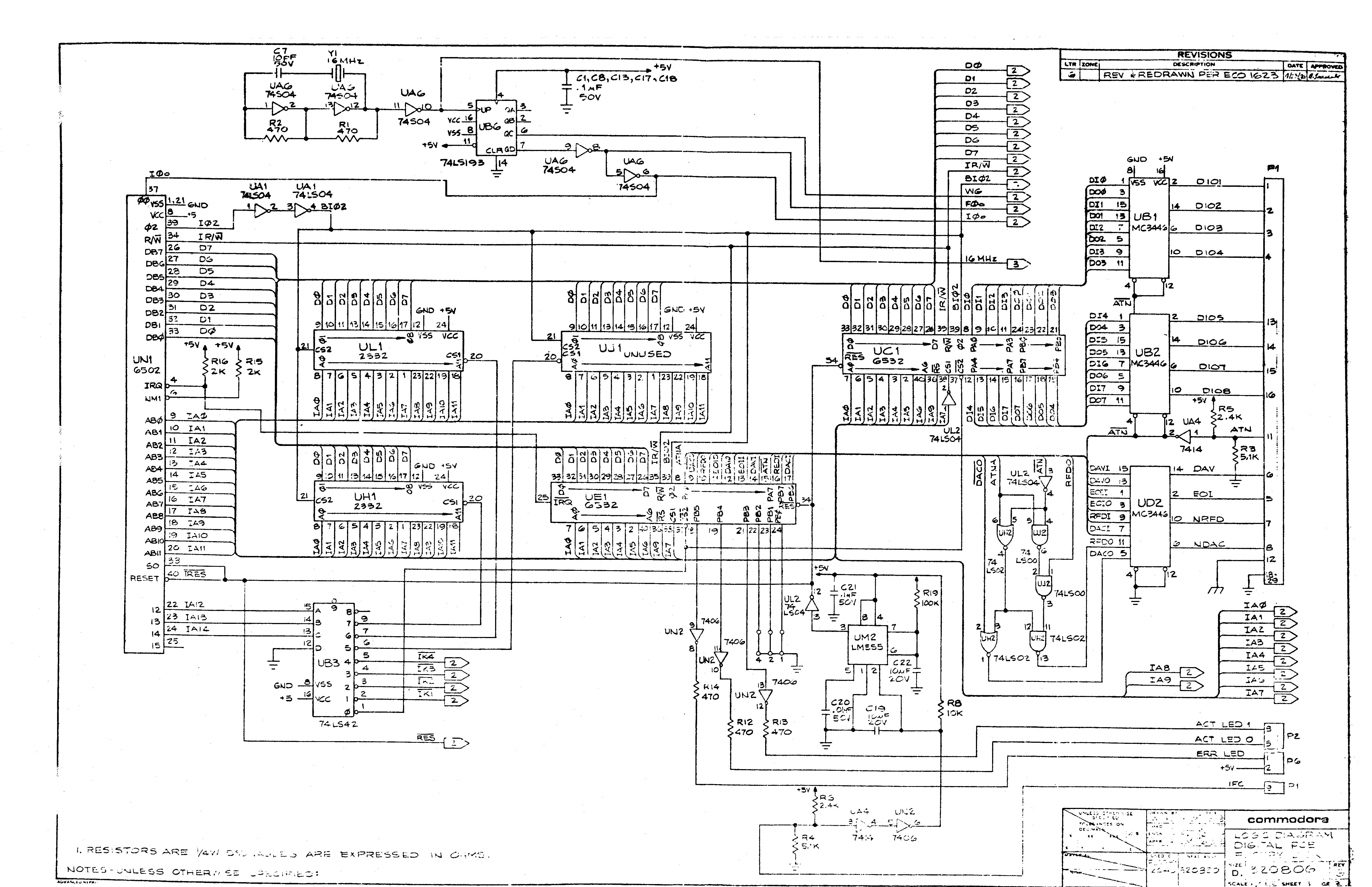
BigEd wrote:
The 74LS02 is a TTL part, a quite different process. Actually I'm not sure how good TTL is at pulling all the way up to the rail, but maybe it's fine.
TTL does a very poor job of pulling up, but pullup resistors offer a (somewhat inelegant) solution. You'll see power-wasting, low-value pullups on the 74ls02 circuit that generates Φ1 and Φ2 on the 6509-based CBM machine. (Nowadays an 'AC02 would be a much better choice.)

Hobbit1972 wrote:
does V also travel the other way round? Could the state of V be measured at SO?
No, SO is strictly an input. Interesting idea, though.

Hobbit1972 wrote:
Or to put it a little differently and look at the uses of SO:

wait on some external event - time critical: I could use RDY instead, which would give an even faster response. [...]
It's true there are alternatives to using SO -- indeed, the alternatives proved far more popular!

BigEd wrote:
Moto's later improved chip, the 6809, was initially the same idea as the 6800 - an external clock generator. But the B version needs only a single clock, IIRC.
Yes, Ed - the 6809 (not to be confused with 6509) was avaiable in external-clock versions. But these were designated by an "E" suffix on the part number. Codes such as A B C indicated the speed rating (not the external clock).

cheers
Jeff

_________________
In 1988 my 65C02 got six new registers and 44 new full-speed instructions!
https://laughtonelectronics.com/Arcana/ ... mmary.html


Top
 Profile  
Reply with quote  
PostPosted: Thu Jun 25, 2015 4:41 pm 
Offline
User avatar

Joined: Thu Dec 11, 2008 1:28 pm
Posts: 10802
Location: England
Oh, yes, 6809E - I remember now!

You are of course quite right about needing pads - the drivers for an output pad are about as big as the pad itself.

I've just looked at the top edge of the 6502/6501 schematics. I see these pads:
nmi
(vma) (n.c. on 6502) (sync on 6509, whereas sync pin, not on top edge, is used for AEC)
irq
clkout/phi1 (missing on 6509)
rdy
vss (missing on 6509 - power is near pin 8)
vss (double pad) (this position used for phi2 in on 6509)
res
clk2out/phi2 off (used for phi1 in on 6509?)
so/c.p.s. (missing on 6509)
clk0/phi2 (missing on 6509)
cclk/dbe (n.c. for 6502) (missing on 6509)
[no pad, corresponds to n.c. on 6502]
rw

Having looked that up, I belatedly notice that SO and P1-P4 are not on the top edge at all, but on the bottom edge, between D7 and A15. It's possible that D4,5,6 and 7 pads have been used for these pins, and D0-D7 have been routed up and round the corner. That's already true for D0 on the 6502 - the pad is some way from the driver. It won't hurt much, as external capacitances and delays will be much greater, I think, than the on-chip. In fact there's a fossil of a different arrangement, as D1 is pointlessly taken up to right next to the D0 pad:
http://visual6502.org/JSSim/expert.html ... 0&zoom=1.7


Top
 Profile  
Reply with quote  
PostPosted: Fri Jun 26, 2015 4:33 am 
Offline

Joined: Sun Oct 14, 2012 7:30 pm
Posts: 107
All of the CBM disk drives used the SO pin, connected to the data separator. When a byte of data has been converted from flux to GCR, the SO pin goes low which sets bit 6 (V) of the flags. This has to be cleared in software (CLV) or you won't see the next one occur. This was used from the late 70's (PET drives) until the early 90's when CBM stopped producing the 1571.

I know this quite well, because it is what I am currently working on - a cycle exact CBM disk drive emulator using a PIC micro. I am emulating the 6502, two 6522's, 2K of RAM, and the data separator hardware with the proper crazy memory map that mirrors and has invalid (undecoded) addressing.


Top
 Profile  
Reply with quote  
PostPosted: Fri Jun 26, 2015 5:04 am 
Offline
User avatar

Joined: Thu May 28, 2009 9:46 pm
Posts: 8190
Location: Midwestern USA
Dr Jefyll wrote:
Hobbit1972 wrote:
wait on some external event - time critical: I could use RDY instead, which would give an even faster response. [...]

It's true there are alternatives to using SO -- indeed, the alternatives proved far more popular!

If you can afford to stall out the system for a short period of time, the SEI -- WAI sequence on the WDC MPUs produces single cycle response time to an IRQ or NMI. Both Garth and I describe it in our interrupt articles.

_________________
x86?  We ain't got no x86.  We don't NEED no stinking x86!


Top
 Profile  
Reply with quote  
PostPosted: Fri Jun 26, 2015 5:40 am 
Offline
User avatar

Joined: Tue Feb 10, 2015 5:27 pm
Posts: 80
Location: Germany
JimDrew wrote:
All of the CBM disk drives used the SO pin, connected to the data separator. When a byte of data has been converted from flux to GCR, the SO pin goes low which sets bit 6 (V) of the flags. This has to be cleared in software (CLV) or you won't see the next one occur. This was used from the late 70's (PET drives) until the early 90's when CBM stopped producing the 1571.

I know this quite well, because it is what I am currently working on - a cycle exact CBM disk drive emulator using a PIC micro. I am emulating the 6502, two 6522's, 2K of RAM, and the data separator hardware with the proper crazy memory map that mirrors and has invalid (undecoded) addressing.


This is... interesting. Schematics for 4040 show that SO is pulled up, no connection to data seperator:
http://www.zimmers.net/anonftp/pub/cbm/schematics/drives/old/4040/320806-1.gif

and ROM code doesn't use SO therefore:
Code:
 FDB1  24 4D     iFDB1      BIT VIA_IFR    ; get the bytes, store in (BUFPT),y, update checksum, jmp DEND
 FDB3  10 FC                BPL iFDB1
 FDB5  A5 41                LDA VIA_DIN
 FDB7  91 16                STA (BUFPT),Y
 FDB9  45 08                EOR WORK
 FDBB  85 08                STA WORK
 FDBD  C8                   INY
 FDBE  D0 F1                BNE iFDB1


"Byte ready" is tested via VIA. GCR decoding fully done in hardware. Checksum is generated within the loop.
Source: http://www.6502.org/users/andre/petindex/drives/roms/dos1fdc.html


SO came into use in later series, 8250 for sure (didn't check with 8050 yet):
Code:
FD9F          LFD9F:
FD9F 50 FE      BVC LFD9F
FDA1          LFDA1:
FDA1 B8         CLV
FDA2 A5 41      LDA io_diskdata_read_fdc
FDA4 91 17      STA (bufpnt_fdc),Y
FDA6 C8         INY
FDA7 D0 F6      BNE LFD9F


The guess would be that someone miscalculated the time available: 8250 has a higher data rate -- but still would leave plenty of time to do it the old way (no SO, test via VIA, checksum calculated later in a second loop), but the someone thought there would not be that plenty of time and tried to cut corners.


Last edited by Hobbit1972 on Fri Jun 26, 2015 5:57 am, edited 2 times in total.

Top
 Profile  
Reply with quote  
PostPosted: Fri Jun 26, 2015 5:53 am 
Offline
User avatar

Joined: Tue Feb 10, 2015 5:27 pm
Posts: 80
Location: Germany
BigDumbDinosaur wrote:
If you can afford to stall out the system for a short period of time, the SEI -- WAI sequence on the WDC MPUs produces single cycle response time to an IRQ or NMI. Both Garth and I describe it in our interrupt articles.


You could get the same latency single cycle by using RDY. For NMOS read access/all CMOS accesses that should be even faster than WAI:
Code:
;WDC:
SEI
start_hardware_we_want_to_access
WAI
LDA result_of_hardware

;RDY
start_hardware_we_want_to_access
LDA result_of_hardware; hardware stalls CPU on read till ready

Using RDY would be 2 clocks faster for it is already waiting inside the LDA. Using WAI would have to load LDA instruction, address byte (and possibly second address byte if I/O not in ZP).

On CMOS this works the same with writes. NMOS CPU would be a bit trickier to implement for write cycles don't care about RDY there.


Top
 Profile  
Reply with quote  
Display posts from previous:  Sort by  
Post new topic Reply to topic  [ 22 posts ]  Go to page 1, 2  Next

All times are UTC


Who is online

Users browsing this forum: No registered users and 2 guests


You cannot post new topics in this forum
You cannot reply to topics in this forum
You cannot edit your posts in this forum
You cannot delete your posts in this forum
You cannot post attachments in this forum

Search for:
Jump to: