AndrewP wrote:
Cookie13! wrote:
Attachment:
The attachment Address decoder.xlsx is no longer available
I'm not familiar with Ben Eater's 6502 memory map but I must say the interactive spreadsheet is pretty sweet

His memory map is from Garth Wilson's single IC address decoder circuit:
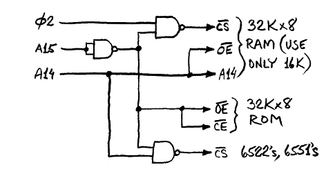
https://wilsonminesco.com/6502primer/addr_decoding.htmlSee below for the image from:
https://wilsonminesco.com/6502primer/32 ... Mlogic.jpgIt inverts A15 with one NAND gate, and that is fed into /ROM_CS and /ROM_OE (using leading "/" to mean active low), so /ROM_CS and /ROM_OE are active low from $8000-$FFFF.
/ROM_CS := /ROM_OE := NAND(A15,A15)
It selects a 32K SRAM when A15 is low and Phi2 is high by taking that inverted A15 and combining it with Phi2 so that SRAM is only selected in the second half of the clock phase:
/RAM_CS := NAND(Phi2,NAND(A15,A15))
It feeds A14 into the /RAM_OE, so RAM only outputs in $0000-$3FFF, using 16KB of the 32KB RAM. Note that /RAM_OE is also active low in $8000-$BFFF, but in that range RAM is not selected.
/RAM_OE := A14
It derives the /IO_SELECT by taking the NAND of A14 and the inverted 15 line, so /IO_SELECT is active low in $4000-$7FFF:
/IO_SELECT := NAND(A14,NAND(A15,A15)
Then it can take advantage of 6502 bus I/O chips like the VIA that have two selects, one active low and one active high, by tying one of the address lines from A8-A13 to the active high select and /IO_SELECT to the active low select.
You are free to extend that down to up to 10 "slots" with A0-A3 for register addressing, but with such a massive I/O memory mapped space available, using A8-A13 means that the device is the first two digits of a hexadecimal address and the register address in the device is the second two digits.
You avoid the problem that an address like $7F04 (%01.111111.00000100) would select all of the I/O device by "don't do that" ... you only use addresses with one of the address lines A8-A13 high:
%01.000001 = $41 ... Device0 = $40+2^0
%01.000010 = $42 ... Device1 = $40+2^1
%01.000100 = $44 ... Device2 = $40+2^2
%01.001000 = $48 ... Device3 = $40+2^3
%01.010000 = $50 ... Device4 = $40+2^4
%01.100000 = $60 ... Device5 = $40+2^5
If you want to put an active low shift register or a latch in that I/O address you can use a couple of NAND gates for active low:
/IO5 := NAND(A13,NAND(/IOSELECT,VCC))
A single quad NAND could put three single active low select parts on Device3-Device5 that way. Or you can also fit a single active low select part as Device5 and a single active high part as Device4:
/IO4 := NAND(A12,NAND(/IOSELECT,VCC))
IO4 := NAND(/IO4,VCC)
Garth also has a version of a single chip Address Decode for 32KB of RAM from $0000-$7FFF, IO in $8000-$BFFF, and 16KB of ROM in $C000-$FFFF. With that one, if you have a 32KB ROM, you can put the ROM A14 line on a jumper between VCC and GND and have two different ROM banks ... you could even dedicate a VIA GPIO to ROM A14 and have software selectable ROM banks. IMHO, that one is more interesting for a Forth system, since I would like to have a Kernel jump table to load and save RAM images and common I/O routines and core primitives I am not going to monkey around with in the ROM and a (separated header) Forth dictionary in RAM, so I would have more code in RAM than is common with Ben Eater's "reprogram the ROM and see what happens" approach.


