6502.org Forum  Projects  Code  Documents  Tools  Forum
It is currently Sat Apr 27, 2024 6:24 pm

All times are UTC


Post new topic Reply to topic  [ 15 posts ] 
Author Message
PostPosted: Thu Jul 06, 2023 10:18 am 
Offline
User avatar

Joined: Mon Aug 30, 2021 11:52 am
Posts: 251
Location: South Africa
Why's this under programming? I'm not sure if I understand JML on the 65816. I think even in emulation mode it can be used to change the program bank register; if not then my memory map below falls apart.

I had a fairly normal 6502 style memory map going on. The first low 32KB mapped as RAM, the next 32KB mapped as ROM and devices sandwiched in at 00:7000. The great thing about that memory map is the reset vector can point to program code in the ROM space. Bog standard stuff. Then I allowed writes to RAM in ROM space and finally turned off ROM decoding making everything in bank zero RAM.

Now I'm wondering why?

If I (magically) have the reset vector pointing to 00FFF0 and magically make the 4 bytes starting at 00FFF0 encode the instruction JML $24_bit_address then I effectively have reset vector than can be outside of bank 0.

This opens up the following, pretty cool, memory map:
Attachment:
Memory Map.png
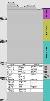
Memory Map.png [ 91.46 KiB | Viewed 6188 times ]


That gives me 8 banks of RAM using a 512KB AS7C34096-8 SRAM and also 512KB of ROM using a SST39LF040-55 Flash. And makes address decoding a lot simpler.

Except for the 16 bytes jammed at the top of bank zero.

Be that as it may it can be decoded and those addresses can be sent off to a CPLD (like the ATF16V8) or even a diode ROM.

Just wondering if this is a complete brainfart or if it seems workable.

Cheers!
Andrew


Last edited by AndrewP on Thu Jul 06, 2023 6:55 pm, edited 3 times in total.

Top
 Profile  
Reply with quote  
PostPosted: Thu Jul 06, 2023 11:02 am 
Offline
User avatar

Joined: Wed Feb 14, 2018 2:33 pm
Posts: 1399
Location: Scotland
It's your system, so build it as you want it....

All you have to do is write the code - the monitor, OS, utilities, etc. ...

Or you look at existing systems and think you might want to do it in a way that might work with them - maybe to make writing the code for the monitor/os etc. easier... Only you can make that decision.

I made the decision to not have any ROM, have a small 256 byte window for IO (Just one VIA) at $FExx and in the '816 system 512KB of RAM. I also made the decision that all directly executable code would live in bank 0. This has not been an issue for me so-far.

That lets me run BBC Basic (and others) in 6502 mode and my BCPL OS in native mode. (The BCPL bytecode can live anywhere in the memory map...

So maybe have a think (or a re-think?) about what the plans are for software before you lift the soldering iron...

-Gordon

_________________
--
Gordon Henderson.
See my Ruby 6502 and 65816 SBC projects here: https://projects.drogon.net/ruby/


Top
 Profile  
Reply with quote  
PostPosted: Thu Jul 06, 2023 12:00 pm 
Offline
User avatar

Joined: Thu Dec 11, 2008 1:28 pm
Posts: 10793
Location: England
(AFAICT JML will indeed jump to a 24 bit address and therefore set K, the bank register, accordingly. Note that in 6502 mode an interrupt will only stack two bytes of PC, so you mustn't take interrupts while running in a high bank, unless you take steps to record the bank yourself.)


Top
 Profile  
Reply with quote  
PostPosted: Thu Jul 06, 2023 12:24 pm 
Offline
User avatar

Joined: Mon Aug 30, 2021 11:52 am
Posts: 251
Location: South Africa
Thanks, that's good point about being able to use existing code and resources.

I find myself in a bit of a weird space. I'd already been designing (simulating really) my system for a bit more than a year before my first post on this forum. And before that I'd never done any significant electronics project. At the time of my first post I'd already largely settled on a design. And that design is ... peculiar ... compared to most of the 65xx computers I've seen built on this forum. In some ways it's kinda outsider art, I started the hardware design side blind but have a pretty deep knowledge of software design. And that shows; both in my assumption I'd be writing all the software from scratch and in how 'incompatible' it is with everything existing.

It wasn't even a choice; just flow of circumstance.

An example would be DOS65. Probably a good choice for 65xx based system but by the time I'd noticed it I'd already written and pretty thoroughly tested a FAT32 filesystem. And that's supposed to be running off of a SD card running in high speed SD mode (something I should be testing right now but am avoiding - but it mostly seems to work). My strange asymmetric clock choice gives me some unusual DMA options. The SD card can transparently read into memory byte-by-byte at the '816s clock frequency. Which makes for some interesting programming possibilities. But the counter to this is that none of the software I've written is lightweight. My FAT32 implementation isn't.

A decision I'm making now (but not quite) is that the whole of bank zero should probably become Direct Page 'register' like memory and stack. Anyone's thoughts on that be appreciated as that's late breaking and not properly considered.

And whilst typing this I see BigEd has posted (thanks!) that JML will work as long as I kick the '816 into native mode before any interrupts occur. Which should be fine as the only interrupt I can get is the NMI watchdog. And that timer resets on system reset and only first ticks 500 µs afterwards.


Top
 Profile  
Reply with quote  
PostPosted: Thu Jul 06, 2023 3:56 pm 
Offline
User avatar

Joined: Thu May 28, 2009 9:46 pm
Posts: 8144
Location: Midwestern USA
Succinctly, all 65C816 instructions are functional in either mode.

That said, some are of minimal value in emulation mode, MVN and MVP being two of them. Also, as Ed notes, you have to be cautious with using JML and JSL in emulation mode, due to PB not being preserved during an interrupt. In emulation mode, it isn’t possible to select 16-bit register widths, you’re stuck with a one-page stack hard-wired to $0100, you have to differentiate between an IRQ and BRK, etc. I personally see little reason to run the 816 in emulation mode—doing so is a waste of the MPU’s capabilities.

_________________
x86?  We ain't got no x86.  We don't NEED no stinking x86!


Top
 Profile  
Reply with quote  
PostPosted: Thu Jul 06, 2023 5:28 pm 
Offline
User avatar

Joined: Sun Jun 30, 2013 10:26 pm
Posts: 1927
Location: Sacramento, CA, USA
BigDumbDinosaur wrote:
I personally see little reason to run the 816 in emulation mode—doing so is a waste of the MPU’s capabilities.

You underestimate the value (at least to a certain class of users) of trillions of bytes of legacy code. :)

_________________
Got a kilobyte lying fallow in your 65xx's memory map? Sprinkle some VTL02C on it and see how it grows on you!

Mike B. (about me) (learning how to github)


Top
 Profile  
Reply with quote  
PostPosted: Thu Jul 06, 2023 6:11 pm 
Offline
User avatar

Joined: Mon Aug 30, 2021 11:52 am
Posts: 251
Location: South Africa
I'm definitely in the put-it-in-native-mode-and-leave-it-there camp. But then I guess I would be :D

Anyway I managed to break WinCupl (who knows how) and no amount of clean installing will make it work again so instead of using an ATF16V8 (or 22V10) I decided to try building the address decode and data bus in Logisim.
Attachment:
Reset Long Vector.png
Reset Long Vector.png [ 46.72 KiB | Viewed 6133 times ]

It wasn't so bad and will probably be about 10 ICs (including logic gates). It should play nicely in a 20 to 25MHz system. The biggest downside is that the 74LVC16244s are 0.5mm pitch TSSOP48 ICs and those don't solder without a fight.

Not much else to add other than that I found this to be a fun exercise and maybe I will actually try this memory layout; it simplifies a lot of the other complicated address decoding I had. Only time, lots more time, will tell.


Top
 Profile  
Reply with quote  
PostPosted: Thu Jul 06, 2023 10:11 pm 
Offline
User avatar

Joined: Sat Jul 24, 2021 1:37 pm
Posts: 282
An alternative solution to encoding a JML with a CPLD / diode ROM would be to mirror the ROM in bank 0. You could make $00FFE0-00FFFF and for example $08FFE0-$08FFFF both trigger the ROM's Chip Select.

Alternatively, you could start your 512k of ROM at $008000 and end at $087FFF, making it aligned to half banks.

I'm designing a future hypothetical computer around this idea, by mirroring RAM to low bank 0, and by allowing ROM to grow past bank 0 in a continuous way. This still gives emulation mode a 32/32 split of bank 0, while allowing full access to both chips in a continuous way in native mode. Note that in the binary image of the ROM, the first 32k will actually be accessible at the end of the range by the computer.

Code:
/* Address decoding */

FIELD ADDRESS = [A0..23];

RAM_CS  = ADDRESS:[000000..007DFF] # ADDRESS:[090000..10FFFF]; // 512k or RAM starting at bottom half of bank 9, with first ~32k mirrored in bottom half of bank 0 (minus I/O)
ROM_CS  = ADDRESS:[008000..087FFF]; // 512k of ROM starting at top half of bank 0

IO_CS0  = ADDRESS:[007E00..007EFF]; // 256B
IO_CS1  = ADDRESS:[007F00..007FFF]; // 256B


Or you could mirror both ROM and RAM so memories are bank aligned in native mode in this scheme

Code:
RAM_CS  = ADDRESS:[000000..007DFF] # ADDRESS:[090000..10FFFF];
ROM_CS  = ADDRESS:[008000..00FFFF] # ADDRESS:[010000..08FFFF];

_________________
BB816 Computer YouTube series


Top
 Profile  
Reply with quote  
PostPosted: Fri Jul 07, 2023 1:04 am 
Offline
User avatar

Joined: Thu May 28, 2009 9:46 pm
Posts: 8144
Location: Midwestern USA
barrym95838 wrote:
BigDumbDinosaur wrote:
I personally see little reason to run the 816 in emulation mode—doing so is a waste of the MPU’s capabilities.

You underestimate the value (at least to a certain class of users) of trillions of bytes of legacy code. :)

Actually, I don’t. Almost all “legacy” code will run just fine in the 816’s native mode. Exceptions include use of undefined opcodes and dependency on quirks peculiar to the eight-bit processors, e.g., zero page wrap and the NMOS behavior of JMP (<addr>).

When I permanently switched POC V1.0 from emulation to native mode operation, I initially didn’t do anything to the firmware, except to add CLC - XCE to the startup. :D

_________________
x86?  We ain't got no x86.  We don't NEED no stinking x86!


Top
 Profile  
Reply with quote  
PostPosted: Fri Jul 07, 2023 1:08 am 
Offline
User avatar

Joined: Thu May 28, 2009 9:46 pm
Posts: 8144
Location: Midwestern USA
AndrewP wrote:
Anyway I managed to break WinCupl (who knows how) and no amount of clean installing will make it work again...

Try combing through the Windows registry for anything related to WinCUPL and delete it. Needless to say, making a backup copy of the registry is a good idea before you go on your slash-and-burn expedition. :D

_________________
x86?  We ain't got no x86.  We don't NEED no stinking x86!


Top
 Profile  
Reply with quote  
PostPosted: Fri Jul 07, 2023 12:34 pm 
Offline
User avatar

Joined: Mon Aug 30, 2021 11:52 am
Posts: 251
Location: South Africa
akohlbecker wrote:
An alternative solution to encoding a JML with a CPLD / diode ROM would be to mirror the ROM in bank 0. You could make $00FFE0-00FFFF and for example $08FFE0-$08FFFF both trigger the ROM's Chip Select.
That is a very good idea and one that seems obvious in hindsight :oops: I already have the RAM deslected at that point, it would be really easy to enable the ROMs select for those addresses.

And even the clock stretching just works because it is based on the ROM select line.

BigDumbDinosaur wrote:
Try combing through the Windows registry for anything related to WinCUPL and delete it.
:? I :? hate :? Windows :?

I've cleared out everything even vaguely WinCupl related but no joy. It seems to be related to the project file GUI - just the GUI. If I delete every generated file then I get one compile before it breaks again. I really need to move to GALasm or something.


Top
 Profile  
Reply with quote  
PostPosted: Fri Jul 07, 2023 2:18 pm 
Offline
User avatar

Joined: Fri Aug 03, 2018 8:52 am
Posts: 745
Location: Germany
if the GUI is the issue, couldn't you just use the underlying commandline programs? so far i've found that much more usable.
also not sure if windows is to blame if the program is like 30 years old at this point. i'm honestly suprised the GUI is sometimes functional at all!


Top
 Profile  
Reply with quote  
PostPosted: Fri Jul 07, 2023 7:17 pm 
Offline
User avatar

Joined: Thu May 28, 2009 9:46 pm
Posts: 8144
Location: Midwestern USA
AndrewP wrote:
:? I :? hate :? Windows :?

You are not alone, my friend. :D

_________________
x86?  We ain't got no x86.  We don't NEED no stinking x86!


Top
 Profile  
Reply with quote  
PostPosted: Mon Jul 10, 2023 1:02 am 
Offline

Joined: Fri Apr 15, 2016 1:03 am
Posts: 136
Here is another simple fast option for getting RESET code out of the flash memory.

The 65816 requires a bank address latch to get the hi address bits.
A method to modify the bank address bits with zero additional delay is to tri-state off the bank address latch outputs & tri-state on a reset bank address buffer to put a fixed bank address on the bus.

The 65816 reset sequence would be:
--- Hardware RESET asserted.
This sets the "reset mode addressing" flip-flop.
This disables the bank address latch outputs & enables the reset bank address buffer outputs.
This maps the reset bank of the flash memory into every CPU bank.
--- Hardware RESET released, 65816 reset sequence starts.
The RESET vector is fetched from the reset flash memory bank.
A JML instruction is executed from the reset flash memory bank to set the CPU's program bank.
A read-modify-write instruction is executed from the reset flash memory bank.
--- The read-modify-write generates a pulse on the 65816 ML (memory lock) line.
This clears the "reset mode addressing" flip-flop.
This disables the reset bank address buffer outputs & enables the bank address latch outputs.
Address mapping is now normal.
The CPU is executing out of the reset flash memory bank.

If bank zero is all RAM:
All of the 65816 interrupt vectors point to RAM at the top of bank zero.
The program executing in the reset flash memory bank could copy some data from flash memory to bank zero RAM to simulate some ROMs being mapped into bank zero.
I/O could be mapped into its own bank to simplify RAM address decoding.

Sample memory map:
$000000..$3fffff: RAM
$400000..$7fffff: more RAM
$800000..$bfffff: I/O (decoded further)
$c00000..$ffffff: Flash memory


Top
 Profile  
Reply with quote  
PostPosted: Mon Jul 10, 2023 1:46 pm 
Offline
User avatar

Joined: Mon Aug 30, 2021 11:52 am
Posts: 251
Location: South Africa
leepivonka wrote:
Here is another simple fast option for getting RESET code out of the flash memory.
That's an even better idea, thanks! And that reduces my address decode to enable ROM from is address in interrupt vector space to just is addressing ROM mode flip-flop set.

Proxy wrote:
if the GUI is the issue, couldn't you just use the underlying commandline programs?
Yup, they still work pretty well!


Top
 Profile  
Reply with quote  
Display posts from previous:  Sort by  
Post new topic Reply to topic  [ 15 posts ] 

All times are UTC


Who is online

Users browsing this forum: No registered users and 31 guests


You cannot post new topics in this forum
You cannot reply to topics in this forum
You cannot edit your posts in this forum
You cannot delete your posts in this forum
You cannot post attachments in this forum

Search for:
Jump to:  
cron