6502.org Forum  Projects  Code  Documents  Tools  Forum
It is currently Fri May 10, 2024 1:06 am

All times are UTC


Post new topic Reply to topic  [ 51 posts ]  Go to page Previous  1, 2, 3, 4
Author Message
 Post subject: Re: Macro help?
PostPosted: Thu Mar 24, 2022 9:20 pm 
Offline
User avatar

Joined: Thu Mar 24, 2022 8:52 pm
Posts: 10
My I answer on this old thread? I even registered here in order to add what I have to say. ;)

I stumbled about the WDTEST macro myself some days ago, and I tried to do my own investigations.

I wrote my findings an guesses on the cbm-hackers mailing list (cf. http://www.softwolves.com/arkiv/cbm-hac ... 1585.html; unfortunately, many of the postings on this list were very OT), and I want to give the results here:

My first post was (http://www.softwolves.com/arkiv/cbm-hac ... 31585.html):

Quote:
I am trying to understand the sources of the 1571 and 1581 drives.

In the original drive sources of the 1571 and 1581 (as found on
zimmers.net), there is a macro WDTEST:

Code:
WDTEST  .macro
        .ife <*!.$03
        nop
        .endif
        .endm

I am not completely familiar with the syntax of the assembler used, but
if I understand it correctly, it issues a NOP if bit 0 and bit 1 of the
PC are both 0 - that is, the PC address is divisble by 4.

The (incomplete) listing at
http://www.zimmers.net/anonftp/pub/cbm/ ... serlib.zip seems to
confirm my assumption.


This macro is always used before the WD177x status is read (lda, bit) or
stored to the same address (WD177x command register). That is, it is
always similar to this:

Code:
        WDTEST          ; chk address
cmd7    lda  wdstat


So, can anyone think of a reason WHY it is done this way? I cannot think
of a reason why this NOP would be needed in some cases, and why it
depends upon the address bits.

I have thought if there might be a problem if the PC is divisible by 4,
because of the sequence of the bus operation of the 6502? That is, could
it be that the WD177x accidiantially recognises a read of the DATA
register, and there would be data loss?

What do I mean?

The 6502 absolute addressing is as follows (looking into the MOS 6502
programming manual, appendix E.3):

Code:
Clock    Adress Bus      PC      DAta bus    comments
Cycle     
  1        PC           PC + 1    OP CODE    fetch op code
  2        PC + 1       PC + 2    ADL        fetch ADL
  3        PC + 2       PC + 3    ADH        fetch ADH
  4        ADH,ADL      PC + 3    Data       fetch Data
  5        PC + 3       PC + 4    OP CODE    fetch new op code, execute old op cod

Now, if in cycle 4, there would be a glitch in that the ADH is already
correct, but the ADL is not yet there (but, instead, PC+3 would be
output), this might be a read (or write) to the data register of the
WD1772.

I know, this is a VERY wild guess, and I cannot think that this problem
would only occur in the 157x and 158x drives, but also with other
peripheral devices (like CIA, PIA, VIA, ...). Unfortunately, other than
that, I cannot think of any reason for these NOP.

---------------------------

Then, Francesco/Frank answered with another wild guess, saying that it might be related to using the "wrong" clock PHI1 instead of PHI2 (http://www.softwolves.com/arkiv/cbm-hac ... 31586.html):

Quote:
wild guess:
The WD1770 in the Commodore 1571 (and I guess in the 1581 too, but
I've never seen one) has its chip select line
qualified with the wrong clock. Let me explain better: when a
peripheral device must be connected to the 6502's bus, it either has a
phi2 input
or we usually qualify the select to happen during phi2 high.
Sometimes, for example with static rams, it's usually enough to
qualify the write signal to phi2 high only.
Now, the 1571 was made when all the good engineers had already left
Commodore by a long time and to save one gate, they used phi1 LOW
OR'ed with the decoded
address range to obtain the WD1770 select.
Phi1 and phi2 aren't an inverted replica of each other. The low phase
of phi1 is LARGER than the high phase of phi2 and phi2's low phase is
larger than phi1 high phase,
that's to avoid any possible bus contention if devices use phi1 and
phi2 HIGH phases to access the same bus (like on the old dual cpu
drives for example).
Now, if one uses phi1 as "poor man's" inverted phi2, it turns out that
the chip select to the WD1770 might happen too early (phi2 not yet
high) and cause unpredictable
behaviour.
Since also the WD1770 need two address lines and they are supplied by
A0 and A1, it was probably wise to never have both A0 and A1 both low
just before a real access
to this device, since its chip select has the wrong timing and maybe
A0=A1=0 was the worst possible fake access to this device.
However, they should have corrected the hardware, not make this
software workaround.
VIA/PIA and all other native 6502 peripherals have a phi2 input, so
the address decode glue logic need not worry about qualifying the
selects against phi2 high phase.


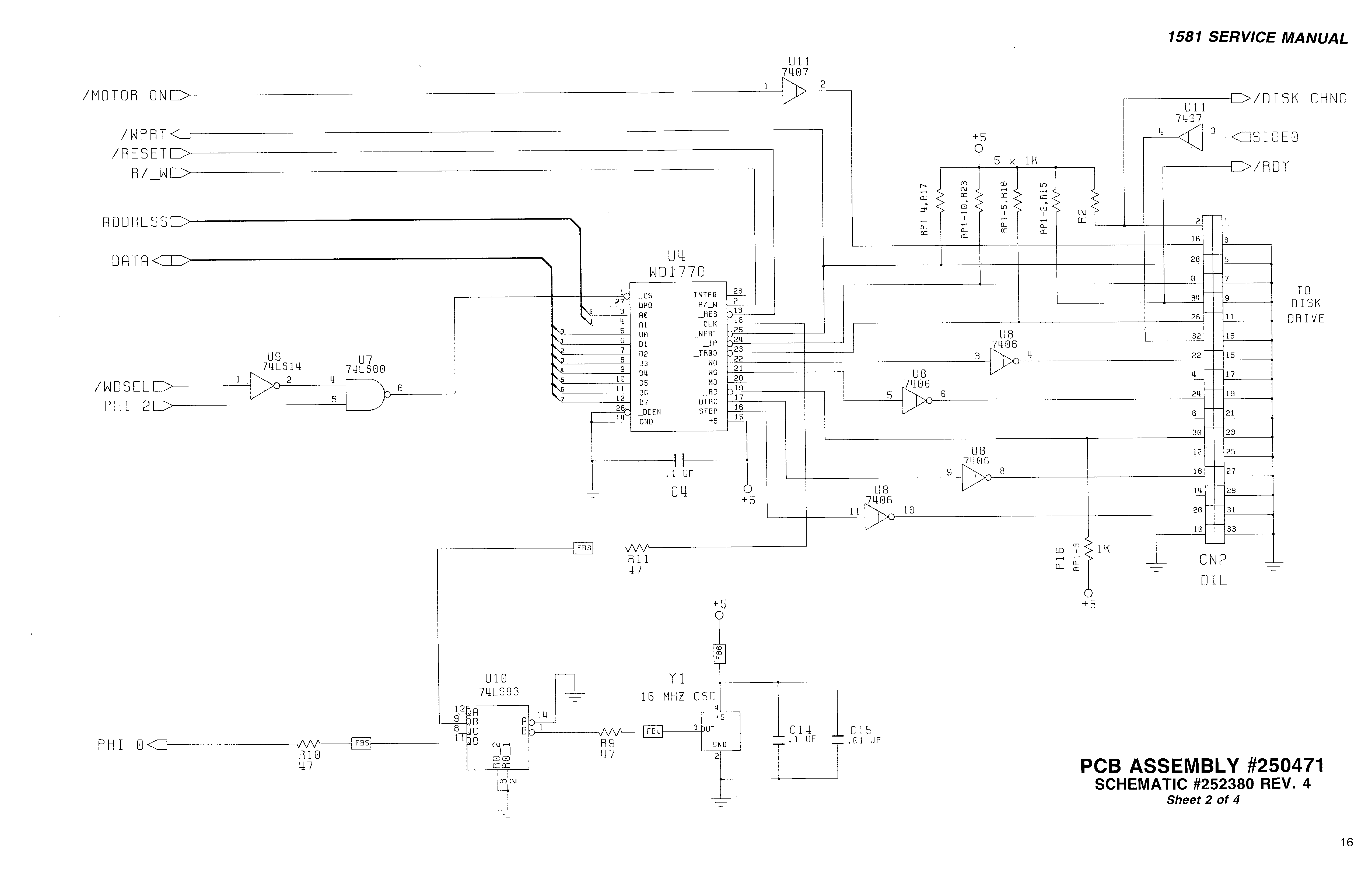
I said it doesn't make sense, because the -CS of the WD177x is wired to PHI2 (cf. http://www.softwolves.com/arkiv/cbm-hac ... 31591.html), and it was confirmed by Gerrit Heitsch (in http://www.softwolves.com/arkiv/cbm-hac ... 31592.html).


Now, I believe I was wrong and I looked into the wrong floppy drive! I believe this is a problem of the 1571 only, not of the 1581! This might explain why the tests made above did not show any result!

I wrote the following (cf. http://www.softwolves.com/arkiv/cbm-hac ... 31638.html):

Quote:
As the code is already there with the 1571, it might be a hardware
glitch that was to be prevented that does not exist on the 1581. Or it
might be something that happens very seldom.

I looked at the data sheets of the WD1770/WD1772, the 6502 and the
schematics of the 1581:

The -CS for the WD177x is generated as: -CS = -(PHI2 AND NOT -WDSEL)
(cf.
http://www.zimmers.net/anonftp/pub/cbm/ ... 581-16.gif)
with a 74LS00,
and

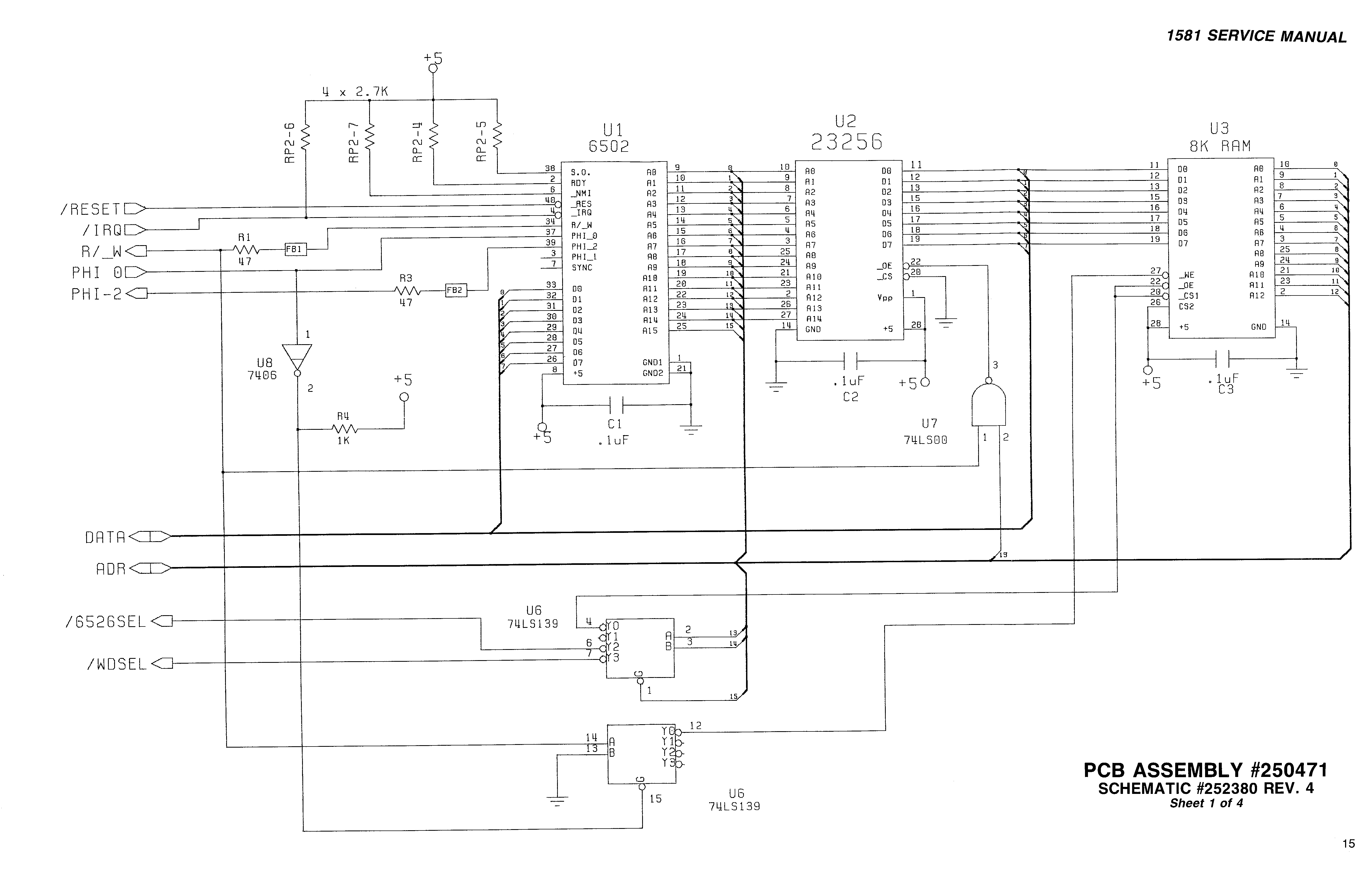
-WDSEL = is the output of a 74LS139 decoder with A13=A14=1 and A15=0),
connected directly to the 6502 output (cf.
http://www.zimmers.net/anonftp/pub/cbm/ ... 581-15.gif)

So, the -CS is gated directly with PHI2 through a 74LS00. The maximum
propagation delay of it is 15 ns.

For the WD177x, T_AH (address hold after -CS is going high) is minimum
10 ns.

For the 6502, the t_ADH (address hold after PHI2 falls) is minimum 30 ns.

Thus, when PHI2 falls, at most 15 ns later, -CS is de-asserted. Thus,
t_ADH of the 6502 guarantees that it will be stable for at least 15 ns,
which is enough for the T_AH of the WD177x.

I do not see any problems with this on the 1581.


For the 1570/1571, it is different (cf. marked schematics at
in the attachment):

The -CS of the WD177x is generated through a 74F32 (a 2-Input OR gate)
and pin 17 (-CS1) of the 20 pin gate array (marked in red), and PHI1 (!
- marked in green).


So, it seems that the "wild guess" of Frank is right! I did not find any
numbers in the 6502 data sheet of when PHI1 goes high after PHI2 goes
low, but it seems to be later than PHI2. It must be later, because
otherwise, PHI1 and PHI2 would be overlapping.

So, the time to react for the -CS of the WD177x is shortened. This might
explain why Commodore used a 74*F*32, which has a shorter propagation
delay (max of around 7 ns) than a 74LS32 or 74LS00, but it could be that
this is still not enough!


This would explain why the tests of the forum.6502.org thread did not
show any bad effect when the NOP was removed: On the 1581, it seems not
to be critical, but on the 1570/1571, it might be critical!


Now, I think you are more knowledgeable on the 6502 than I am. Does anyone know how long the delay of the PHI1 going high after PHI2 going low? The data sheet only says "0 ns min." for "Delay between PHI1 and PHI2", which does not help much.

Of course, even if it is a problem, it might not be a problem with all 1570/1571 drives.


Attachments:
File comment: 1571 Schematic with the inputs to the -CS of the WD177x marked
1571-wd177x.png
1571-wd177x.png [ 2.32 MiB | Viewed 592 times ]
Top
 Profile  
Reply with quote  
 Post subject: Re: Macro help?
PostPosted: Thu Mar 24, 2022 9:27 pm 
Offline
User avatar

Joined: Thu Dec 11, 2008 1:28 pm
Posts: 10800
Location: England
(Welcome! Thanks for popping over and summarising the findings in that thread... which I was vaguely following. However, I don't think I have any answers for you.)


Top
 Profile  
Reply with quote  
 Post subject: Re: Macro help?
PostPosted: Tue Mar 29, 2022 2:52 am 
Offline
User avatar

Joined: Tue Mar 05, 2013 4:31 am
Posts: 1373
Well, nice to see an update on this thread. As for the 1571 being affected and the 1581 not being affected, I can easily say that's not the case. The 1581 will fail if you assemble and link the BIOS without the WDTEST macro.

In short, the macro simply ensures that either A0 and/or A1 are active before accessing the base address of the WD1772 FDC. I'm still nor sure why, but that appears to be the case. If you look at the listing file after the code is assembled and linked, you will find that in every instruction that accesses the status register ($6000), either A0 and/or A1 is active (high). In some cases either one will be active and even both active. In short, the macro will trigger based on the lower 2-bits of the address. Perhaps another way to look at this is: every time the status register is accessed, either A0 and/or A1 must be switched from active to inactive. Also note that the PH2 clock is used as part of the chip select for the WD1772.

I'm just guessing at this point, but it would suggest that there is some unusual timing for the based address, which is the status register. Other registers for the FDC don't use the macro preceding the access, so that seems to imply that's it's specific to an odd internal timing of accessing the status register. I would also note that the hardware interrupt from the WD1772 is not used, nor is the DRQ line, so the chip is only operated in polled I/O mode. Interestingly, the Motor drive line is also not used, as that line to the drive is driven from the 8520.

I guess one could track down Fred Bowen (the guy who wrote the 1581 code) and ask him... last I checked, he did have a LinkedIn profile.

_________________
Regards, KM
https://github.com/floobydust


Top
 Profile  
Reply with quote  
 Post subject: Re: Macro help?
PostPosted: Thu Mar 31, 2022 12:47 am 
Offline
User avatar

Joined: Fri Dec 11, 2009 3:50 pm
Posts: 3354
Location: Ontario, Canada
Welcome, strik. :) Thanks for bringing our attention back to this issue, and for sharing some of the content from the recent cbmhackers thread. Here on 6502.org this intriguing little mystery hasn't received any attention since 2017, and I've just finished reviewed the entire thread in order to refresh my memory.

Although the investigation got set aside before any conclusion was reached, looking back I feel confident I was hot on the trail of the explanation. Although this remains to be proven, I am perhaps supported by some of Francesco's remarks which you quoted, although he's coming at the thing from a different direction. Frank seems cautious about his observation (calling it a "wild guess"), and I too am unsure what to think. If the low phase of Phi1 is larger (ie, wider) than the high phase of Phi2 then it would begin slightly too early and it would also end slightly too late.

strik wrote:
Then, Francesco/Frank answered with another wild guess, saying that it might be related to using the "wrong" clock PHI1 instead of PHI2 (http://www.softwolves.com/arkiv/cbm-hac ... 31586.html):

Quote:
wild guess:
The WD1770 in the Commodore 1571 (and I guess in the 1581 too, but I've never seen one) has its chip select line qualified with the wrong clock. [...] Phi1 and phi2 aren't an inverted replica of each other. The low phase of phi1 is LARGER than the high phase of phi2 [...] Now, if one uses phi1 as "poor man's" inverted phi2, it turns out that the chip select to the WD1770 might happen too early (phi2 not yet high) and cause unpredictable behaviour.


I'm not ready to specifically blame the "poor man's inverted phi2" but I will say there's a convincing explanation of why the floppy system will fail if the FDC Chip Select goes inactive too late. What'll happen is, the FDC will remain selected during a fraction of the CPU's next cycle (as it fetches the next opcode). In other words, the FDC will experience a rogue read.

So, why does the macro care so much about the two LS address bits? It's because the location in memory of the LDA wdstat instruction will determine which FDC register experiences the spurious touch. :!:

The LDA wdstat instruction takes four cycles, and then the CPU proceeds to fetch the next opcode. Here are those five cycles:
    1. ROM access: read the LDA opcode
    2. ROM access: read the LDA LS operand byte
    3. ROM access: read the LDA MS operand byte
    4. FDC access: read register "rr" <== (rr is the reg we intend to read)
    5. ROM access: fetch the next opcode. Early in this cycle is when the rogue read of the FDC occurs.

... and, according to the location in memory of the LDA instruction, here are four possible scenarios for the two LS address bits during the five cycles in question:
    1. 00,01,10,rr,11 <== rogue read of the Data Reg :!:
    2. 01,10,11,rr,00 <== rogue read of the Status Reg
    3. 10,11,00,rr,01 <== rogue read of the Track Reg
    4. 11,00,01,rr,10 <== rogue read of the Sector Reg

What we see here is, only if the LDA opcode is at binary xxx00 will the rogue read touch the FDC Data Register. And AIUI, the Data Reg is read sensitive, whereas rogue reads of the other three FDC addresses produce no significant side effects and can be tolerated. This explains why they created a macro to prevent the LDA opcode from residing at binary xxx00.


In 2017 I posted some experimental hardware hacks intended to correct the problem and thus verify the theory. The hacks involved adding a transparent latch that'd prevent the FDC from receiving the updated A1 and A0 that appear during the opcode fetch. But Francesco's remarks have inspired me to consider mods to the clock signal instead -- an easier approach.

Said mods could take various forms, and although they're fairly simple I'll make them the subject of a separate post. The goal is to ensure the FDC gets deselected earlier so it doesn't see the A1, A0 values associated with the opcode fetch. Comments and suggestions welcome.

-- Jeff

_________________
In 1988 my 65C02 got six new registers and 44 new full-speed instructions!
https://laughtonelectronics.com/Arcana/ ... mmary.html


Top
 Profile  
Reply with quote  
 Post subject: Re: Macro help?
PostPosted: Thu Mar 31, 2022 1:56 am 
Offline
User avatar

Joined: Tue Mar 05, 2013 4:31 am
Posts: 1373
I also spent some time over the past few nights digging into this. I also grabbed some schematics for the Atari ST machines, which also use the WD1772 controller. With the Atari machines, all of the CPU interface lines are connected to their DMA controller, including the data and address lines, R/W, DRQ and CS. Granted, no real knowledge or info on Atari's DMA chip (custom chip), but it does give them absolute control and timing for all registers in the FDC.

I would also reference the WD datasheet, which is not all that great to be honest. It's a bit odd that they don't show any address lines on Read Timings to the FDC, yet they show address lines on Write Timings to the FDC, odd.

Based on everyone's recent input, I would tend to take a different approach for accessing the WD1772. WD did what I would call a half-a** approach to a Motorola 6800 interface (as there's no clock line), so the clock qualification has to happen outside the chip. I would think that isolating the address lines from the address bus and only having them driven when truly selected could in fact be a fix. I'm thinking this is what Atari is doing by having all host interface signals managed by their DMA controller and never being connected to the actual CPU bus. This eliminates any timing anomalies between the various CPU cycles.

To address this (pun intended), either a few gates might be added, or just use a PLD and replace more of the existing circuitry as well... things like all memory and I/O decoding, qualified read and write signals for memory and managing the address lines along with the chip select for the WD1772.

Lastly, I would note that the 1581 drive does not use the PH1 signal from the CPU. PH2 is used for the FDC CS qualification however (and the clock line to the 8520 CIA), and the main CPU clock is used via a 7406 inverter for driving the half of the 74LS139 to generate a qualified write signal for the 8KB SRAM.

Now I need to think if it would be reasonably easy (without hacking the 1581 PCB) to implement such a fix.... hmmm, some more nights ahead on digging.

_________________
Regards, KM
https://github.com/floobydust


Top
 Profile  
Reply with quote  
 Post subject: Re: Macro help?
PostPosted: Mon Apr 25, 2022 2:39 am 
Offline
User avatar

Joined: Tue Mar 05, 2013 4:31 am
Posts: 1373
All,

Jeff (Dr Jefyll) and I have had some PM going on over the past month or so related to this. Jeff has suggested that the timing is too slow for the /CS line and suggested replacing the 74LS00 with a faster chip (74AHCT00).

A few years back, I took my second 1581 drive and removed all of the chips, capacitors and can oscillator from the PCB. I cleaned out all of the holes, installed new caps and a full set of high quality Mill-Max sockets. I then used new 74HCT logic chips, a new 8KB SRAM and a Rockwell R65C02P4 CPU. The only chips that were kept were the 8520A CIA and the Western Digital WD1772-PH floppy controller. Well, even with the faster HCT logic, there was no difference. The WDTEST Macro was still required! Jeff's suggestion of getting even faster chips was noted (and added to my existing Mouser order).

I opted to do some additional testing... my first 1581 (which is a higher serial number than the first) has a VLSI 1772-02 floppy controller (soldered in). Some years ago, I ordered a few NOS VLSI1772-02 FDCs (which were licensed by WD) and also picked up a few of the Atari made chips, which support the higher data rates for the HD diskettes. I opted to install a VLSI chip, modified the source code and commented out the WDTEST macro. To my surprise, the drive still works... and I've done significant testing over the past few days on this. Note: The Atari controller also works fine in the drive. If replace either the 74HCT139 or 74HCT00 with the original LS parts, the drive eventually fails.

This does highlight that early WD1772-PH controllers have some internal timing problems. It would appear that these were likely corrected when they brought out the WD1772-02 (and even later -02-02) parts, which also have high performance digital data separators. Still, the datasheet is identical to the initial version... so nothing to suggest there is any difference, but there certainly is.

I think Jeff had the right idea... and it seems to be the case. I've added some faster logic chips to my existing shopping list, and at some point, I'll perform additional testing and see if it's possible to have the WD1772-PH controller work without the macro as well... but it will likely be a while... just not sure.

As for my current source code, I've done a fair amount of work on it. It now uses several CMOS opcodes and addressing modes, has sorted out the correct stepping rates for the Chinon drive, integrated the patches implemented in the -02 ROM version, fixed a bug in a routine where the stack wasn't getting pulled properly and I fixed the init code for the ROM checksum so it's working again. The same goes for the Signature 16-bit ROM check. I also changed the ROM version to -03 and the 1581 DOS version to 10C (C for requiring a CMOS CPU).

Attachment:
1772-FDCs.jpg
1772-FDCs.jpg [ 236.7 KiB | Viewed 411 times ]


Hope some others find this useful. At some point (more testing to be done) I'll post the updated source code and -03 ROM image, so others can also update their 1581 if desired.

_________________
Regards, KM
https://github.com/floobydust


Top
 Profile  
Reply with quote  
Display posts from previous:  Sort by  
Post new topic Reply to topic  [ 51 posts ]  Go to page Previous  1, 2, 3, 4

All times are UTC


Who is online

Users browsing this forum: No registered users and 5 guests


You cannot post new topics in this forum
You cannot reply to topics in this forum
You cannot edit your posts in this forum
You cannot delete your posts in this forum
You cannot post attachments in this forum

Search for:
Jump to: