6502.org Forum  Projects  Code  Documents  Tools  Forum
It is currently Sun Apr 28, 2024 11:28 pm

All times are UTC


Post new topic Reply to topic  [ 8 posts ] 
Author Message
PostPosted: Thu Dec 08, 2022 4:56 pm 
Offline
User avatar

Joined: Wed Feb 13, 2013 1:38 pm
Posts: 586
Location: Michigan, USA
What instructions can I use to set a VIA output pin low and then high with the shortest possible time between the low and high transitions, please? I will study the Datasheet but thought I might ask here as well.

I'd like to determine the RC time constant (tau) I'll need on a little 2-pin LCD backpack to be able to drive an HD44780 type LCD from a 1-MHz 6502 through a VIA chip. Backpack diagram and example Arduino program below to show how I use the backpack on PIC and Arduino systems.

TIA. Happy Holidays. Mike

Attachment:
LCD Backpack.png
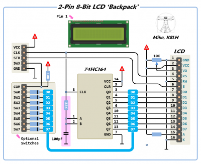
LCD Backpack.png [ 171.09 KiB | Viewed 1343 times ]

Attachment:
rc timing.png
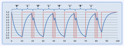
rc timing.png [ 17.81 KiB | Viewed 1392 times ]

Code:
  /******************************************************************
   *  Mike McLaren's 2-pin 8-bit 74HC595/74HC164 LCD Backpack Demo  *
   *                                                                *
   *  16-Sep-18    Arduino 1.8.6 / Arduino Nano                     *
   ******************************************************************/

   #define line1 (0x80+0x00)    // set DDRAM command + line 1 address
   #define line2 (0x80+0x40)    // set DDRAM command + line 2 address
   #define line3 (0x80+0x14)    // set DDRAM command + line 3 address
   #define line4 (0x80+0x54)    // set DDRAM command + line 4 address

   char Scramble [] = "AAAAAAAAA";
   
   #define cbi(sfr, bit) (_SFR_BYTE(sfr) &= ~(1<<bit))  // clear bit
   #define sbi(sfr, bit) (_SFR_BYTE(sfr) |= 1<<bit)     // set bit

  /******************************************************************
   *                                                                *
   ******************************************************************/

   #define clk PORTC2           // 'clk' on PC2 (A2) pin
   #define lat PORTC3           // 'lat' on PC3 (A3) pin

   class LCD : public Print
   { public:                    //
       void init();             //
       void cmd(uint8_t);       //
       size_t write(uint8_t);   //
     private:                   //
       bool rs = 0;             // lcd 'rs' flag
   };

   void LCD::init ()
   { DDRC = 1<<clk|1<<lat;      // make 'clk' and 'lat' outputs
     cbi(PORTC,lat);            // lat = 0
     sbi(PORTC,clk);            // clk = 1
     _delay_ms(100);            // LCD power-on delay
     cmd(0x38);                 // 8-bit, 2-lines, 5x7 font
     cmd(0x0C);                 // display on, cursor & blink off
     cmd(0x06);                 // cursor inc, shift off
     cmd(0x01);                 // clear display
     _delay_ms(2);              // required delay
   }                            //

   size_t LCD::write (uint8_t work)
   { uint8_t bitctr = 8;        //
     uint8_t SaveSREG = SREG;   //
     do                         // start of bit clock cycle
     { if(!(work & 128))        // if b7 is a '0' bit
         cbi(PORTC,clk);        // start clock cycle for a '0'
       _delay_us(9);            // charge or drain cap to 3t
       cli();                   // interrupts off
       cbi(PORTC,clk);          // start clock cycle for a '1'
       sbi(PORTC,clk);          // clock out the '0' or '1'
       SREG = SaveSREG;         // restore SREG & irq enable bit
       work <<= 1;              // prep for next bit
     } while(--bitctr);         // until all 8 bits clocked out
     if(!rs) cbi(PORTC,clk);    // make clk pin = rs flag
     sbi(PORTC,lat);            // latch 595 & pulse LCD 'E' pin
     cbi(PORTC,lat);            //  "
     sbi(PORTC,clk);            // always leave clk pin high
     return 1;                  //
   }                            //

   void LCD::cmd (uint8_t c)
   { rs = 0; write(c); rs = 1;  //
   }                            //

  /******************************************************************
   *  main                                                          *
   ******************************************************************/

   LCD lcd;                     // create instance 'lcd' of LCD class

   int main()                   //
   {
     lcd.init();                // 8-bit mode, cursor inc & off
  /*                                                                *
   *  send a couple 'flash string helper' strings                   *
   *                                                                */
     lcd.print(F("K8LH Backpack")); // (44) 1st instance
     lcd.print(F(" v2"));           // (16) 2nd instance

     lcd.cmd(line2+2);          // line 2, tab 2 (6 bytes)
     lcd.print(Scramble);       // (40 bytes) 1st instance
     lcd.cmd(line2+1);          // line 2, tab 1 (6 bytes)
     lcd.print(Scramble);       // (8 bytes) 2nd instance

     while(1)                   // loop forever
     {                          //
     }                          //
   }                            //


Last edited by Michael on Fri Dec 09, 2022 3:47 am, edited 1 time in total.

Top
 Profile  
Reply with quote  
PostPosted: Thu Dec 08, 2022 9:36 pm 
Offline

Joined: Fri Apr 15, 2022 1:56 pm
Posts: 45
Location: San Antonio, TX, USA
Michael wrote:
What instructions can I use to set a VIA output pin low and then high with the shortest possible time between the low and high transitions, please?
Unless the VIA is mapped into zero page (not common) I think the shortest time will be 4 cycles, i.e. 4 microseconds at 1 megahertz. For example:
Code:
LDA #low_value
LDX #high_value
SEI ; Prevent (maskable) interrupts from interfering with the timing
STA output_register ; 4 cycles
STX output_register ; 4 cycles
CLI


Top
 Profile  
Reply with quote  
PostPosted: Thu Dec 08, 2022 10:48 pm 
Offline
User avatar

Joined: Fri Aug 30, 2002 1:09 am
Posts: 8428
Location: Southern California
What I've done for the clock output of bit-banging SPI is to put it on bit 0 of a port, then use INC and DEC.  Although it's not as fast as pjdennis' way, it leaves the registers available for other things, and you know anyway which way it is so you don't cause it to affect other bits, ie, by INC'ing it when bit 0 is a 1, or DEC'ing it when bit 0 is a 0.

If you just want to put out a square wave without babysitting it, you can use a free-running T1 time-out to toggle PB7, up to half the Φ2 rate.  You'll need the 2 msb's of the 6522's ACR to be 11.

_________________
http://WilsonMinesCo.com/ lots of 6502 resources
The "second front page" is http://wilsonminesco.com/links.html .
What's an additional VIA among friends, anyhow?


Top
 Profile  
Reply with quote  
PostPosted: Fri Dec 09, 2022 3:31 am 
Offline
User avatar

Joined: Wed Feb 13, 2013 1:38 pm
Posts: 586
Location: Michigan, USA
Thank you for the suggestions and insights, guys. I'm not really bit-banging SPI or looking for a square wave. Rather, I'm using a single pin to provide the shift register 'clock' and 'data' signals using an RC Integrator. That same pin also provides the LCD 'RS' signal and a second pin is used to drive the LCD 'E' input. The method is a hybrid bit-banged serial of sorts and I'm just trying to determine the RC values I need for the 'backpack' and the timing requirements to use it on a 6502 system.

Thanks, guys. Happy Holidays.


Top
 Profile  
Reply with quote  
PostPosted: Sat Dec 10, 2022 4:05 pm 
Offline
User avatar

Joined: Wed Feb 14, 2018 2:33 pm
Posts: 1399
Location: Scotland
It's a fascinating example of economy - and I presume you have a vested interest in using/re-using the same "backpack" in several projects - hope it works well. Might make a good thing to publish here for others if there is interest?

As an aside, at 1Mhz you may be able to connect those displays directly to the CPU data bus, RS to A0 and E to a decoded output in a suitable range - you might even want to use R/W rather than software delay for various display operations.

But saying that, I've always connected them to an 8-bit output port on a VIA or '573 latch,

-Gordon

_________________
--
Gordon Henderson.
See my Ruby 6502 and 65816 SBC projects here: https://projects.drogon.net/ruby/


Top
 Profile  
Reply with quote  
PostPosted: Tue Dec 13, 2022 6:32 am 
Offline
User avatar

Joined: Fri Dec 11, 2009 3:50 pm
Posts: 3349
Location: Ontario, Canada
Michael wrote:
What instructions can I use to set a VIA output pin low and then high with the shortest possible time between the low and high transitions, please?
You already have some good suggestions. But if you're really desperate for it to be fast, you should perhaps look into using the Shift Register, outputting in free-run mode onto CB2. In free-run mode the Shift Reg advances once every two clocks, so that's a pretty speedy rate.

In free-run mode, the Shift Reg contents keep recirculating indefinitely, so by loading it with 0 you can make CB2 permanently low, and loading it with $FF will make CB2 permanently high. And I suppose with some fussing you could arrange to output a pulse. For example, if the reg has been full of 0 for a while, you could write a 1 to the reg (or 2, or 4, or 8 etc), wait about 16 cycles or less until the pulse has been output, then set the reg back to 0. I think you get the idea.

Whether the fuss justifies the rather drastic speed increase is up to you. But off the top of my head I think it would work... ! :)

-- Jeff

_________________
In 1988 my 65C02 got six new registers and 44 new full-speed instructions!
https://laughtonelectronics.com/Arcana/ ... mmary.html


Top
 Profile  
Reply with quote  
PostPosted: Tue Dec 13, 2022 8:49 am 
Offline

Joined: Tue Sep 03, 2002 12:58 pm
Posts: 293
This is not a practical solution for the broader problem of communicating with a display in an otherwise usable system. But if you want the shortest possible pulse width from a 6502, here's my impractical solution:

Connect the VIA's RS0-RS3 to the 6502's A1-A4. This way, each register appears duplicated in two consecutive memory locations. Map it somewhere in page 1. Then set the stack pointer to point to the higher of the two data register locations and JSR from a suitable place in memory. When the return address is pushed, the high and low bytes will be written to the data register on two consecutive cycles. With this, you can arrange for a pulse one cycle wide.


Top
 Profile  
Reply with quote  
PostPosted: Wed Dec 14, 2022 1:44 am 
Offline
User avatar

Joined: Wed Feb 13, 2013 1:38 pm
Posts: 586
Location: Michigan, USA
Thank you for stimulating the synapses with some fascinating and innovative ideas...

Happy Holidays, guys...


Top
 Profile  
Reply with quote  
Display posts from previous:  Sort by  
Post new topic Reply to topic  [ 8 posts ] 

All times are UTC


Who is online

Users browsing this forum: No registered users and 28 guests


You cannot post new topics in this forum
You cannot reply to topics in this forum
You cannot edit your posts in this forum
You cannot delete your posts in this forum
You cannot post attachments in this forum

Search for:
Jump to: