6502.org Forum  Projects  Code  Documents  Tools  Forum
It is currently Mon Apr 29, 2024 5:14 pm

All times are UTC


Post new topic Reply to topic  [ 44 posts ]  Go to page Previous  1, 2, 3
Author Message
PostPosted: Sat Apr 06, 2024 2:47 pm 
Offline
User avatar

Joined: Wed Feb 14, 2018 2:33 pm
Posts: 1399
Location: Scotland
rob42 wrote:
to add: I see the same thing, when I run the 6502 at 10Hz. Is that still too slow?


My understanding is that 200Khz is about as slow as the old parts can go, however when building my 6507 system on breadboard I was curious to see if it would run at 2Mhz after running very well at 1Mhz, so I put a 2Mhz oscillator on the breadboard and just moved the wire over.

It carried on working as if nothing had happened, but now at 2Mhz. I switched between 1 and 2Mhz a few times and even left it stopped for a few seconds to see what would happen but to my surprise - nothing. It just stopped then started again.

This is just one data point and it was a slightly newer Rockwell 6507, so who knows.

-Gordon

_________________
--
Gordon Henderson.
See my Ruby 6502 and 65816 SBC projects here: https://projects.drogon.net/ruby/


Top
 Profile  
Reply with quote  
PostPosted: Sat Apr 06, 2024 3:26 pm 
Offline
User avatar

Joined: Fri Dec 11, 2009 3:50 pm
Posts: 3349
Location: Ontario, Canada
rob42 wrote:
The first thing I'll like to eliminate, is that fact that the 'A' register may not be having the value #$FF loaded into it.

Choosing things to eliminate is a good strategy. But I'd say you have already shown that the A register appears to be responding incorrectly. And there are lots of explanations for why this may be -- too many! :shock:

I suggest you change gears, so to speak, and choose for elimination issues that are much more basic. For example, is the chip being supplied with a proper power supply, clock signal and reset signal? (And, related to the clock signal, we need to ascertain whether chip is actually NMOS -- a 6502 -- or CMOS -- a 65C02.)

I "get" that it has probably been fun experimenting to see what evidence can be collected using the methods you find comfortable and familiar. And it's a hobby, so amusing yourself is OK. :) But if it's actual progress you want, then I think it's time to set aside your present tactics and instead review the basics. That's because the "evidence" you're presently collecting may be flawed.

Can you share a photo of your setup? Breadboards can be troublesome, even for seasoned veterans. Also please provide a schematic, or at least a circuit description which briefly mentions every CPU input and what attaches to it; likewise every CPU output and what attaches to it. (But you don't need to individually describe the pins of the address bus -- just a single comment for all 16 is OK. Likewise with the data bus.)

-- Jeff

_________________
In 1988 my 65C02 got six new registers and 44 new full-speed instructions!
https://laughtonelectronics.com/Arcana/ ... mmary.html


Top
 Profile  
Reply with quote  
PostPosted: Sat Apr 06, 2024 3:55 pm 
Offline
User avatar

Joined: Mon Apr 01, 2024 9:58 pm
Posts: 24
Location: ZZ9 Plural Z Alpha
drogon wrote:
My understanding is that 200Khz is about as slow as the old parts can go,


Thank you. I take that on board and appreciate your posting that up.

---

@Jeff

(I'll not quote you here, as your post is right above)

It'll take me a while to do that, but I'll get right to it.

Just to say: there's a good possibility that my monitor app is not doing what I think it's doing (hence my thoughts, in my last post). The reason I say this, is because I added a little code that sets all the GIPO pins that I'm using on the Pico for the 6502 data bus, to $FF right before switching those pins into read mode, ready for the 6502 to present its data. And sure enough, what I monitor came back with was $FF and not what I assume that the 6502 is in fact putting out, which, at that stage, should be the contents of the 'A' register.

I do in fact have a 2nd Pico, which I may be able to employ in some way, but that's maybe adding complexity that will only confuse the set up.

I'll be back with some pictures and such, as soon as I get it all together.

Thank you for sticking with me, guys and I trust that you're not too sick of this thread, just yet.


Last edited by rob42 on Sat Apr 06, 2024 8:00 pm, edited 1 time in total.

Top
 Profile  
Reply with quote  
PostPosted: Sat Apr 06, 2024 4:18 pm 
Offline

Joined: Mon Jan 19, 2004 12:49 pm
Posts: 664
Location: Potsdam, DE
(It's always more fun to debug someone else's setup than your own :mrgreen: )

Neil (who should be wiring up a discrete uart receiver, only if he does, dinner won't happen and then there will be shouting and tears before bedtime!)


Top
 Profile  
Reply with quote  
PostPosted: Sat Apr 06, 2024 7:58 pm 
Offline
User avatar

Joined: Mon Apr 01, 2024 9:58 pm
Posts: 24
Location: ZZ9 Plural Z Alpha
Hey guys.

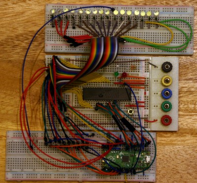
I'm hoping that a picture paints a thousand words and that this will pretty much tell you what you need to know.

Attachment:
IMG_4893.JPG
IMG_4893.JPG [ 1.19 MiB | Viewed 8911 times ]


What is absent here (because I had to move the rig to a different location, in order the photograph it) is the power and ϕ0 IN hook-ups.

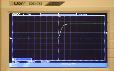
Here, you can see what the ϕ0 IN signal looks like. It's up to TTL logic levels well inside of 50ns (sorry, I've got the scope set at 100ns per division; opps), the peek voltage is 5V and it's a nice clean signal.

Attachment:
IMG_4895.JPG
IMG_4895.JPG [ 1.26 MiB | Viewed 8911 times ]


What else can I tell you? I suppose, if something is not clear, you'll ask me and I can post back. Given time, I'll better understand what you guys need, without you having to ask.

These are medium resolution pictures, as I didn't want to burden the servers with high res, but I think that they should be good enough for you to be able to see enough detail, without a circuit schematic, which would take me hours to prepare, given that I like to have things as good as I can get them, and I've never prepared a schematic before.

If you'd like to see some snippets of the code that's running on the Pico, here is what is most relevant...

This is how I've arranged for the Pico to represent 'memory':

Code:
MEMORY = {
    "FFFF": "00", # IRQ_B (high)
    "FFFE": "00", # IRQ_B (low)
    "FFFD": "06", # RES_B (high)
    "FFFC": "00", # RES_B (low)
    "FFFB": "06", # NMI_B (high)
    "FFFA": "00", # NMI_B (low)
    "0617": "00",
    "0616": "00",
    "0615": "00",
    "0614": "00",
    "0613": "00",
    "0612": "00",
    "0611": "80",
    "0610": "05",
    "060F": "4c", # jmp $8005
    "060E": "60",
    "060D": "00",
    "060C": "8d", # sta $6000
    "060B": "aa",
    "060A": "a9", # lda #$aa
    "0609": "60",
    "0608": "00",
    "0607": "8d", # sta $6000
    "0606": "55",
    "0605": "a9", # lda #$55
    "0604": "60",
    "0603": "02",
    "0602": "8d", # sta $6002
    "0601": "ff",
    "0600": "a9", # lda #$ff
    "01FF": "00", # top of 'the stack'
    "01FE": "00",
    "01FD": "00",
    "01FC": "00",
    "01FB": "00",
    "01FA": "00",
    "01F9": "00",
    "01F8": "00",
    "01F7": "00",
    "01F6": "00",
    "01F5": "00",
    "01F4": "00",
    "01F3": "00",
    "01F2": "00",
    "01F1": "00",
    "01F0": "00",

...

    "010F": "00",
    "010E": "00",
    "010D": "00",
    "010C": "00",
    "010B": "00",
    "010A": "00",
    "0109": "00",
    "0108": "00",
    "0107": "00",
    "0106": "00",
    "0105": "00",
    "0104": "00",
    "0103": "00",
    "0102": "00",
    "0101": "00",
    "0100": "00", # bottom of 'the stack'
    }


That array is accessed with:
Code:
data = MEMORY.get(addr, "EA") # if the memory location is not defined, use 'NOP'
... where addr is the hex value that is read from the address bus. You should be able to see, from the comment, that if an address is not in that array, then data == #$00EA.

Interestingly, while I was contemplating how best to help you guys, to help me, I left my rig running, and I saw that the data write LED (which is the LED on the Pico, as I have this set up: I ran short of GPIO pins, so simply coded the R/W signal to the on-board LED) switching state. Unfortunately, the capture data was lost, but I now have the rig running once again, with the same set up, so I'll let the PC register get up to where I know it was, and post back what I saw.

Tbc...

---

Okay, so something must have been different (but I can't think what) as the R/W signal is now steady. I then remembered that I saw that the address bus was no high than #$00FF (is that the top of what is called 'Zero Page'?) and arranged for that situation to happen, once again. Success! This is what I was seeing, before...

Code:
...

T-State: 250 ..............................
ADDR BUS OUT: 0000|0000|1111|1111 :: 0x00FF
DATA BUS   R: 1110|1010 :: 0xEA

T-State: 251 ..............................
ADDR BUS OUT: 0000|0000|1111|1111 :: 0x00FF
DATA BUS   R: 1110|1010 :: 0xEA

T-State: 252 ..............................
ADDR BUS OUT: 0000|0001|0000|0000 :: 0x0100
DATA BUS   R: 0000|0000 :: 0x00

T-State: 253 ..............................
ADDR BUS OUT: 0000|0001|0000|0000 :: 0x0100
DATA BUS   R: 0000|0000 :: 0x00

T-State: 254 ..............................
ADDR BUS OUT: 0000|0001|0000|0001 :: 0x0101
DATA BUS   R: 0000|0000 :: 0x00

T-State: 255 ..............................
ADDR BUS OUT: 0000|0001|1111|1101 :: 0x01FD
DATA BUS   W: 0000|0000 :: 0x00

T-State: 256 ..............................
ADDR BUS OUT: 0000|0001|1111|1100 :: 0x01FC
DATA BUS   W: 0000|0001 :: 0x01

T-State: 257 ..............................
ADDR BUS OUT: 0000|0001|1111|1011 :: 0x01FB
DATA BUS   W: 0000|0010 :: 0x02

T-State: 258 ..............................
ADDR BUS OUT: 1111|1111|1111|1110 :: 0xFFFE
DATA BUS   R: 0000|0000 :: 0x00

T-State: 259 ..............................
ADDR BUS OUT: 1111|1111|1111|1111 :: 0xFFFF
DATA BUS   R: 0000|0000 :: 0x00

T-State: 260 ..............................
ADDR BUS OUT: 0000|0000|0000|0000 :: 0x0000
DATA BUS   R: 1110|1010 :: 0xEA

T-State: 261 ..............................
ADDR BUS OUT: 0000|0000|0000|0001 :: 0x0001
DATA BUS   R: 1110|1010 :: 0xEA

T-State: 262 ..............................
ADDR BUS OUT: 0000|0000|0000|0001 :: 0x0001
DATA BUS   R: 1110|1010 :: 0xEA
...


So, at T-State 255 to 257, we see a data write of 00, 01, 02

The next time the program counter reaches #$00FF, it's slightly different:

Code:
...
T-State: 769 ..............................
ADDR BUS OUT: 0000|0000|1111|1111 :: 0x00FF
DATA BUS   R: 1110|1010 :: 0xEA

T-State: 770 ..............................
ADDR BUS OUT: 0000|0000|1111|1111 :: 0x00FF
DATA BUS   R: 1110|1010 :: 0xEA

T-State: 771 ..............................
ADDR BUS OUT: 0000|0001|0000|0000 :: 0x0100
DATA BUS   R: 0000|0000 :: 0x00

T-State: 772 ..............................
ADDR BUS OUT: 0000|0001|0000|0000 :: 0x0100
DATA BUS   R: 0000|0000 :: 0x00

T-State: 773 ..............................
ADDR BUS OUT: 0000|0001|0000|0001 :: 0x0101
DATA BUS   R: 0000|0000 :: 0x00

T-State: 774 ..............................
ADDR BUS OUT: 0000|0001|1111|1010 :: 0x01FA
DATA BUS   W: 0000|0000 :: 0x00

T-State: 775 ..............................
ADDR BUS OUT: 0000|0001|1111|1001 :: 0x01F9
DATA BUS   W: 0000|0001 :: 0x01

T-State: 776 ..............................
ADDR BUS OUT: 0000|0001|1111|1000 :: 0x01F8
DATA BUS   W: 0010|0010 :: 0x22

T-State: 777 ..............................
ADDR BUS OUT: 1111|1111|1111|1110 :: 0xFFFE
DATA BUS   R: 0000|0000 :: 0x00

T-State: 778 ..............................
ADDR BUS OUT: 1111|1111|1111|1111 :: 0xFFFF
DATA BUS   R: 0000|0000 :: 0x00

T-State: 779 ..............................
ADDR BUS OUT: 0000|0000|0000|0000 :: 0x0000
DATA BUS   R: 1110|1010 :: 0xEA

T-State: 780 ..............................
ADDR BUS OUT: 0000|0000|0000|0001 :: 0x0001
DATA BUS   R: 1110|1010 :: 0xEA

T-State: 781 ..............................
ADDR BUS OUT: 0000|0000|0000|0001 :: 0x0001
DATA BUS   R: 1110|1010 :: 0xEA

T-State: 782 ..............................
ADDR BUS OUT: 0000|0000|0000|0010 :: 0x0002
DATA BUS   R: 1110|1010 :: 0xEA
...


... 00, 01, 22

From then on, each time the program counter reaches #$00FF, it's the same as the above: first 00, 01, 02 then 00, 01, 22 and each time, a little lower on the 'stack', so that what has gone before, would not be overwritten.

Now, as you'll see from the coding, I've learned that the 'stack' is from #$0100 to #$01FF (please correct me, if that is not true) and as such, what I think I'm seeing here, is that the 6502 is trying to place those three values onto the 'stack'.

As is, my code (that is to say, my monitor code) is not responding to any data write requests; it's simply monitoring them, but I can (and I plan to) change that, if it becomes worth while.

The point here, is that now I know for sure, that my app is reading the the data bus and not simply echoing what it wrote to the data bus on it last operation: it didn't write anything to the data bus (#$00 aside, which is always there, in the absence of anything else) during this, what I would call, an idle stage.

What do you think?

Again, guys, I can't thank you enough for your help here and I'd like to assure you that I'm not simply wasting your time here; I'm serious about this build. I may be a little unconventional, but I'd like to think, that in the end, I'll have a project that others can learn something from, even if that that 'something', is "Don't do what I've done.".

~ Rob (alias Marvin) :mrgreen:

p.s: I'm still confused about why I didn't see the contents of the 'A' register, before, but maybe you guys can throw some much needed light on that, now that you have something more with which to work.

Thank you very much.


Top
 Profile  
Reply with quote  
PostPosted: Sun Apr 07, 2024 2:06 am 
Offline
User avatar

Joined: Mon Apr 01, 2024 9:58 pm
Posts: 24
Location: ZZ9 Plural Z Alpha
Update:

I've made some real progress with this...

The first task was to ensure that I was getting a sane reading from the 6502 Data Bus. So, I hooked up my scope to 'D0' and 'D1', then set the ASM code to load #$01 then #$02 and finally #$03, in turn, into the 'A' register and with each value, store said at #$0000. The signal returns looked spot on, so from there, I knew it had to be an issue was with my monitor.

After doing a little thinking and reading once again, how the GPIO pins can be configured, I reworked my app, so that the GPIO pins for the data R/W were never floating: I had them pulled down, whenever they were waiting for a data read. I also coded a pin reset function, which is called before either a data read or a data write. That way, I could be sure that whatever was on those pins before, would be cleared before any new operation.

Still, I was seeing no data, when the 6502 was sending data to those pins. So, I set up a loop of 1000 reads, rather than a single read, as I had been doing, reasoning that maybe the data read was over before the 6502 had time to send it, and presto! At apx read 600, there was my missing data! So, the Pico was reading, then moving on WAY too fast, for the slow clock speeds at which I was running the 6502.

Then it hit me: simply have the Pico sit around doing the data read, until the 6502 clock changed its state. Still nothing. So, I used the value #$FF, just to see if that made any difference. And, yes: I saw 0000 1111, so half the data. Coding in two reads per clock pulse, and I saw 1111 1111 -- Bingo!

So, I can run the my 6502 at 2Hz and so long as I slow my monitor app down and read the Data Bus a few times, rather than just the once, I see perfect results, with that very simple ASM code. I've yet to test more complex ASM, as my coding skills with ASM are, well, none existent, tbh.

So, is this the proof that we need to finally ID my 6502?


The monitor trace, so that you can see what I'm seeing (running at 2.000Hz):

Code:
Program start

T-State: 29 ..............................
ADDR BUS OUT: 0000|0110|0000|0000 :: 0x0600
DATA BUS   R: 1010|1001 :: 0xA9             <- LDA

T-State: 30 ..............................
ADDR BUS OUT: 0000|0110|0000|0001 :: 0x0601
DATA BUS   R: 1111|1111 :: 0xFF             <- #$FF

T-State: 31 ..............................
ADDR BUS OUT: 0000|0110|0000|0010 :: 0x0602
DATA BUS   R: 1000|1101 :: 0x8D             <- STA

T-State: 32 ..............................
ADDR BUS OUT: 0000|0110|0000|0011 :: 0x0603
DATA BUS   R: 0000|0010 :: 0x02             <- low byte

T-State: 33 ..............................
ADDR BUS OUT: 0000|0110|0000|0100 :: 0x0604
DATA BUS   R: 0110|0000 :: 0x60             <- high byte

T-State: 34 ..............................
ADDR BUS OUT: 0110|0000|0000|0010 :: 0x6002 <- we're here
DATA BUS   W: 1111|1111 :: 0xFF             <- and we have our #$FF with us

T-State: 35 ..............................
ADDR BUS OUT: 0000|0110|0000|0101 :: 0x0605 <- we're back
DATA BUS   R: 1010|1001 :: 0xA9             <- LDA

T-State: 36 ..............................
ADDR BUS OUT: 0000|0110|0000|0110 :: 0x0606
DATA BUS   R: 0101|0101 :: 0x55             <- #$55

T-State: 37 ..............................
ADDR BUS OUT: 0000|0110|0000|0111 :: 0x0607
DATA BUS   R: 1000|1101 :: 0x8D             <- STA

T-State: 38 ..............................
ADDR BUS OUT: 0000|0110|0000|1000 :: 0x0608
DATA BUS   R: 0000|0000 :: 0x00             <- low byte

T-State: 39 ..............................
ADDR BUS OUT: 0000|0110|0000|1001 :: 0x0609
DATA BUS   R: 0110|0000 :: 0x60             <- high byte

T-State: 40 ..............................
ADDR BUS OUT: 0110|0000|0000|0000 :: 0x6000 <- we're here
DATA BUS   W: 0101|0101 :: 0x55             <- and again, we have our baggage

T-State: 41 ..............................
ADDR BUS OUT: 0000|0110|0000|1010 :: 0x060A <- the PC
DATA BUS   R: 1010|1001 :: 0xA9             <- LDA

T-State: 42 ..............................
ADDR BUS OUT: 0000|0110|0000|1011 :: 0x060B
DATA BUS   R: 1010|1010 :: 0xAA             <- #$AA

T-State: 43 ..............................
ADDR BUS OUT: 0000|0110|0000|1100 :: 0x060C
DATA BUS   R: 1000|1101 :: 0x8D             <- STA

T-State: 44 ..............................
ADDR BUS OUT: 0000|0110|0000|1101 :: 0x060D
DATA BUS   R: 0000|0000 :: 0x00             <- low byte

T-State: 45 ..............................
ADDR BUS OUT: 0000|0110|0000|1110 :: 0x060E
DATA BUS   R: 0110|0000 :: 0x60             <- high byte

T-State: 46 ..............................
ADDR BUS OUT: 0110|0000|0000|0000 :: 0x6000 <- we're here again
DATA BUS   W: 1010|1010 :: 0xAA             <- and again, we have our baggage

T-State: 47 ..............................
ADDR BUS OUT: 0000|0110|0000|1111 :: 0x060F <- the PC
DATA BUS   R: 0100|1100 :: 0x4C             <- JMP

T-State: 48 ..............................
ADDR BUS OUT: 0000|0110|0001|0000 :: 0x0610
DATA BUS   R: 0000|0101 :: 0x05             <- low byte

T-State: 49 ..............................
ADDR BUS OUT: 0000|0110|0001|0001 :: 0x0611
DATA BUS   R: 1000|0000 :: 0x80             <- high byte

T-State: 50 ..............................
ADDR BUS OUT: 1000|0000|0000|0101 :: 0x8005 <- the PC
DATA BUS   R: 1110|1010 :: 0xEA             <- default memory content

T-State: 51 ..............................
ADDR BUS OUT: 1000|0000|0000|0110 :: 0x8006 <- just keep right on going...
DATA BUS   R: 1110|1010 :: 0xEA

T-State: 52 ..............................
ADDR BUS OUT: 1000|0000|0000|0110 :: 0x8006
DATA BUS   R: 1110|1010 :: 0xEA

T-State: 53 ..............................
ADDR BUS OUT: 1000|0000|0000|0111 :: 0x8007
DATA BUS   R: 1110|1010 :: 0xEA

T-State: 54 ..............................
ADDR BUS OUT: 1000|0000|0000|0111 :: 0x8007
DATA BUS   R: 1110|1010 :: 0xEA

T-State: 55 ..............................
ADDR BUS OUT: 1000|0000|0000|1000 :: 0x8008
DATA BUS   R: 1110|1010 :: 0xEA

T-State: 56 ..............................
ADDR BUS OUT: 1000|0000|0000|1000 :: 0x8008
DATA BUS   R: 1110|1010 :: 0xEA

T-State: 57 ..............................
ADDR BUS OUT: 1000|0000|0000|1001 :: 0x8009
DATA BUS   R: 1110|1010 :: 0xEA

T-State: 58 ..............................
ADDR BUS OUT: 1000|0000|0000|1001 :: 0x8009
DATA BUS   R: 1110|1010 :: 0xEA

T-State: 59 ..............................
ADDR BUS OUT: 1000|0000|0000|1010 :: 0x800A
DATA BUS   R: 1110|1010 :: 0xEA
...


As you may be able to guess, I'm very pleased that I was able to get this rig doing something predictable. You guys were a big help and often times (I find) it's not until one explains things to others, that things drop into place and one has an idea about the way to go.

It's about 3am here, so I'll get a few hours sleep and I'll maybe have some more to say soon, but I'll hold off until I have a little feedback from you guys, as maybe you'll have me try something that I've not thought of.

Thanks for reading and for your interest in what I'm doing, as well as your help to get me this far.

~ Rob


Top
 Profile  
Reply with quote  
PostPosted: Sun Apr 07, 2024 4:53 am 
Offline
User avatar

Joined: Fri Dec 11, 2009 3:50 pm
Posts: 3349
Location: Ontario, Canada
rob42 wrote:
I knew it had to be an issue was with my monitor.
Yes, it's important to always remember the possibility that your test setup could be misleading you.

Quote:
After doing a little thinking and reading once again, how the GPIO pins can be configured, I reworked my app, so that the GPIO pins for the data R/W were never floating [...] So, I set up a loop of 1000 reads, rather than a single read, as I had been doing, reasoning that maybe the data read was over before the 6502 had time to send it, and presto!
Presto? Sorry, but I'm not convinced you've arrived at the best solution, or even an OK solution. But luckily there's an easier way.

Isn't it true that the 6502 get its clock from one of your GPIO pins? Because the clock is under your control, there's no need to contrive a time delay. It's much better to simply organize things with a view to how the 6502/65C02's data bus normally functions, as follows:

    - Floating of the data bus is normal and desirable anytime the CPU's clock input is low. :!: During this time, the CPU does not drive the data bus, and neither should the attached device. This is true both for read cycles and for write cycles. (In a real computer the attached device would be memory, but in your case it's the Pico.)

    - for a write cycle, the CPU will start driving write data onto the data bus very soon (approx 100 ns or less) after the CPU's clock input is brought high, and it will stop driving the data bus very soon after the CPU's clock input is brought low. So, it's normal for the memory to accept the data that was present just before the clock was brought low (and your Pico should do the same).

    - for a read cycle, the memory should start driving read data onto the data bus shortly after the CPU's clock input is brought high, and it should stop driving the data bus very soon after the CPU's clock input is brought low. The CPU's internal logic will accept the read data that was present just before the clock was brought low.

Things are done this way because it's important that the CPU and the memory "take turns," and don't ever try to drive the data bus simultaneously. Hope this helps...

-- Jeff

_________________
In 1988 my 65C02 got six new registers and 44 new full-speed instructions!
https://laughtonelectronics.com/Arcana/ ... mmary.html


Last edited by Dr Jefyll on Sun Apr 07, 2024 4:59 am, edited 1 time in total.

Top
 Profile  
Reply with quote  
PostPosted: Sun Apr 07, 2024 4:57 am 
Offline
User avatar

Joined: Fri Aug 30, 2002 1:09 am
Posts: 8428
Location: Southern California
I see Jeff posted while I was writing.  I'll post this anyway.  Do spend some time in the data sheet, including the timing diagrams and charts.  The write data is not put on the bus until tMDS time after Φ2 rises.  That amount of time depends on the part, not the clock frequency.  The processor expects the receiving end to latch it in when Φ2 falls.  When it reads data, it does not need the data right away when Φ2 rises, but expects it to be there at least tDSR time before Φ2 falls.  You mention pull-down resistors.  What resistor value did you use?  Note that NMOS outputs, like TTL and LSTTL, cannot pull up nearly as hard as they can pull down, so it is generally better to have pull-up resistors rather than pull-down.  If there's anything resembling a TTL or LSTTL input connected to a line, getting a valid logic-0 pull-down will require a resistance that's too low for such an output put pull up against to achieve a valid logic-1 level.  If you stick to CMOS parts, there won't be any such problems, and you don't need pull-up or -down resistors.  Parasitic capacitance on each line will hold the last driven logic state for quite a while, at least milliseconds, not just nanoseconds or microseconds, and it's not a problem.  There's no need to clear it between drives, and in fact trying to do so just wastes power.

_________________
http://WilsonMinesCo.com/ lots of 6502 resources
The "second front page" is http://wilsonminesco.com/links.html .
What's an additional VIA among friends, anyhow?


Top
 Profile  
Reply with quote  
PostPosted: Sun Apr 07, 2024 10:35 am 
Offline
User avatar

Joined: Mon Apr 01, 2024 9:58 pm
Posts: 24
Location: ZZ9 Plural Z Alpha
Dr Jefyll wrote:
Presto? Sorry, but I'm not convinced you've arrived at the best solution, or even an OK solution. But luckily there's an easier way.


My punctuation was a little off and I was a tired, so it's not clear, but that sentence is a run-on (I know, it's bad grammar) should be read as: "... and presto! At apx read 600, there was my missing data!". It's not a solution, you're correct, but rather it is (or was) a step in that direction, as I could now see that the data was there all along; I just hadn't timed the reading cycle correctly (yes, Neil, you kind of knew, that the timing was going to be the issue).

Dr Jefyll wrote:
Isn't it true that the 6502 get its clock from one of your GPIO pins?


It was, but that's no longer the case. Back on page two, I mentioned that I had off-loaded the clock signal generation and repurposed the GPIO to read the clock signal, rather than provide it.

This I needed (and wanted) to do, because, although the Pico CPU (the RP2040) is dual core, my Python skills are lacking, when it comes to multi threaded code. The issue with using a single thread, is the fact that, the more I ask the Pico to do, the longer its going to take to cycle the script. And if that script includes supplying the ϕ0 signal, there's going to be a drift in the clock speed/timing, because that operation was being controlled by a simple `sleep(x)` statement. Also, to move this one step closer to the goal, the 6502 needs to be independent of the Pico and more dependent on the hardware that will be in the final build. I've yet to buy a crystal oscillator, but that is on my "to-do" list and I have a very reliable stand-in, to fill the gap.

Thank you for all of the bullet pointed information; it's very helpful, and I'll use that, to improve upon my Pico app.

---

Hey Garth,

I'll not quote you, as your post is right above this one.

Thank you for taking the time and trouble to reply. Your explanation (as with the one from Jeff), has given me a lot of very useful information and, indeed, I should spend way more time reading the data sheet (RTFM, right?).

The 'pull-down' resisters to which I refer, are build-in to the Pico (in fact, my understanding is that they're built-in to the RP2040 CPU) and are software controlled. The documentation that I've read on that, can be found on this link: http://www.d3noob.org/2022/10/pull-up-a ... s-and.html

The reason that I configured my app to pull the GPIO pins low, was down to the fact that I was seeing (or I thought I was seeing) 'ghost data' on those pins, in so much as the data that I saw as coming 'from' the 6502, was in fact the data that had just been sent 'to' the 6502.

Now that I have a better understanding of, not only what I should be doing, but also, how to do that, as well as consistent and predictable readings, I can start to remove functions (such as the one that clears the data bus by pulling the data pins low) that I don't need.

---

My deepest thanks to you both, as well as everyone else that has contributed to this thread.

My next move will be to see just how far I can take this concept and how fast I can run it, but before I can do that, I need to gain some ASM coding skills.

I've had an idea, about how the finished rig may operate, which is to have different EPROMS, for each 'program' that I want to run. Or, maybe, I could have many programs on the one EPROM and a DIP Switch to select which one will run; kind of like the plug-in carts that gaming consoles use, only my cart, will have a DIP switch for the program selector. This is, of course WAY down the road from here, with many, many steps before I get even close to that.


My best regards to all, enjoy your day, and I'll be back to read other threads, as well as monitor this thread, for any more responses.

~ Rob.


Top
 Profile  
Reply with quote  
PostPosted: Sun Apr 07, 2024 2:34 pm 
Offline
User avatar

Joined: Fri Dec 11, 2009 3:50 pm
Posts: 3349
Location: Ontario, Canada
rob42 wrote:
Back on page two, I mentioned that I had off-loaded the clock signal generation and repurposed the GPIO to read the clock signal, rather than provide it.

This I needed (and wanted) to do, because, although the Pico CPU (the RP2040) is dual core, my Python skills are lacking, when it comes to multi threaded code. The issue with using a single thread, is the fact that, the more I ask the Pico to do, the longer its going to take to cycle the script. And if that script includes supplying the ϕ0 signal, there's going to be a drift in the clock speed/timing, because that operation was being controlled by a simple `sleep(x)` statement.

You lost me with "drift." Is it your concern that one clock cycle may end up having a different duration than the one before it? I suspect you may be worrying about things that don't matter. The 6502 doesn't require any consistency from one clock cycle to the next. :wink: The specs only say that each individual cycle is supposed to satisfy certain timing requirements.

Quote:
my Python skills are lacking, when it comes to multi threaded code
Allow me to suggest a single-tasking approach that's compatible with an externally-supplied clock and with the bus protocol bullet points I mentioned above. (And it won't matter if the Pico runs at a gazillion MHz; this will still work.)

For a 65xx read cycle:
    - Pico inputs the Clock signal and keeps resampling until Clk is low.
    - Pico inputs the Clock signal and keeps resampling until Clk is high.
    - Pico un-floats the data bus and outputs data.
    - Pico inputs the Clock signal and keeps resampling until Clk is low.
    - Pico floats the data bus.

For a 65xx write cycle:
    - Pico inputs the Clock signal and keeps resampling until Clk is low.
    - Pico inputs the Clock signal and keeps resampling until Clk is high.
    - Pico inputs what is on the data bus and remembers it (copies it to a variable).
    - Pico inputs the Clock signal. If it is high, Pico jumps back a step and once again copies the data bus to the variable, replacing the variable's previous value. And if Clk is low then the cycle is complete, and the most recent value in the variable is accepted as valid.

BTW, in the photo, I don't see any bypass capacitors located nearby the 6502. It is in your interest to remedy this, as it may be causing trouble we haven't yet pinned down. Signing off for now,

-- Jeff

_________________
In 1988 my 65C02 got six new registers and 44 new full-speed instructions!
https://laughtonelectronics.com/Arcana/ ... mmary.html


Top
 Profile  
Reply with quote  
PostPosted: Sun Apr 07, 2024 3:47 pm 
Offline
User avatar

Joined: Fri Dec 11, 2009 3:50 pm
Posts: 3349
Location: Ontario, Canada
Afterthought: In the last post there's an assumption that, when the cycle begins, you already know whether it's going to be a read or a write. But a real-life memory chip (which is what the Pico is emulating) doesn't initially know. In light of that, here's an update:

All cycles begin as follows:
    - Pico inputs the Clock signal and keeps resampling until Clk is low.
    - Pico inputs the Clock signal and keeps resampling until Clk is high.
    - Pico inputs the R/W line from the 6502.
If R/W is high then a read cycle is indicated:
    - Pico un-floats the data bus and outputs data.
    - Pico inputs the Clock signal and keeps resampling until Clk is low.
    - Pico floats the data bus, and the cycle is complete.
Else if R/W is low then a write cycle is indicated:
    - Pico inputs what is on the data bus and remembers it (copies it to a variable).
    - Pico inputs the Clock signal. If it is high, Pico jumps back a step and once again copies the data bus to the variable, replacing the variable's previous value. And if Clk is low then the cycle is complete, and the most recent value in the variable is accepted as valid.

_________________
In 1988 my 65C02 got six new registers and 44 new full-speed instructions!
https://laughtonelectronics.com/Arcana/ ... mmary.html


Top
 Profile  
Reply with quote  
PostPosted: Sun Apr 07, 2024 4:16 pm 
Offline
User avatar

Joined: Fri Jan 26, 2024 5:47 am
Posts: 37
Location: Prague; Czech Republic; Europe; Earth
rob42 wrote:
And if that script includes supplying the ϕ0 signal, there's going to be a drift in the clock speed/timing, because that operation was being controlled by a simple `sleep(x)` statement.


(I know, that you do not generate the ϕ0 signal anymore, but this may help you next time or with different tasks)

There is a simple trick how to wait without `sleep(x)` and avoid drift:

    fetch current_time to variable stored_time
    loop (forever or so):
      if (current_time - stored_time) > wanted_period
        do your task()
        increase stored_time by wanted_period
    repeat loop

this approach means, that your task is started at regular time (plus minus some jitter), regardless how long it takes to run it (well, it should be less then wanted_period, at least statistically)

also you can have more such tasks in one loop, each with different timing, and simulate easy multitasking this way

(one task for clock, another task for communicating with user (read and debounce keys), another task for simulating external inputs (prepare next character for your simulated Serial input at simulated baud rate), ,...)

Also if the time is just limited (like 16 bit, 32bit or so) and overflows, this order of operations ((current_time - stored_time) > wanted_period) ensures, that it works as well, if same limits are put on the variables (everything is 16bits, or everything is 32bits, or so) and computing (simply subtract it and ignore underlow/overflow)

_________________
http://micro-corner.gilhad.cz/, http://8bit.gilhad.cz/6809/Expanduino/Expanduino_I.html, http://comp24.gilhad.cz/Comp24-specification.html, and many others


Top
 Profile  
Reply with quote  
PostPosted: Mon Apr 08, 2024 1:52 am 
Offline
User avatar

Joined: Mon Apr 01, 2024 9:58 pm
Posts: 24
Location: ZZ9 Plural Z Alpha
Dr Jefyll wrote:
You lost me with "drift."


You could be correct, that I'm overly concerned, but what I was driving at, is that as I add more code to the MicroPython script, said script will take longer to execute, slowing the generated clock pulse; that's the "drift". Like I said, it's no longer an issue, because the Pico is no longer performing that task, so the point becomes moot.

Thank you for the very detailed steps, for my monitor to keep in sync with the 6502. In fact, it's not as complicated as all that: I simply created a small function, that gets called, whenever the monitor needs to know if the 6502 clock state has changed...

Code:
def clock_state_change():
    state_change = CLK_READ.value()
    while CLK_READ.value() == state_change:
        pass
    return


... where `CLK_READ` has been setup as a GPIO `machine.Pin.IN`, which monitors the 6502 ϕ1(OUT) signal.

I've run my rig up to 30Hz plus, but that's where my system hits its limit. That's way too fast for what I'm trying to do, at this stage, in any case.

Dr Jefyll wrote:
BTW, in the photo, I don't see any bypass capacitors located nearby the 6502. It is in your interest to remedy this, as it may be causing trouble we haven't yet pinned down.


I don't fully understand what this means, but I will take steps to find out. I trust that you'll advise me, if I can't figure this out for myself.

I, once again, thank you for your time, your trouble, your excellent input, as well as taking an active interest in what I'm doing. I'm sure that I'll need more help, as I move this project along.

---

@gilhad

Thank you for posting that: your insight and input is very much appreciated.

---

As a general update, I now have my (so called) monitor app, acting as both ROM and RAM, and I've mapped out a small portion of that memory, to act as a I/O, just so that I could have a ASM program run on the 6502 and see some results.

Doing what I've done, in the way that I've done it, makes complete sense to me, and I've learned so much from this, which I see as a firm foundation on which to build.

As has already been suggested, some way back in this thread, I think the next thing I should try, is to single step my 6502. Given that I can capture the steps, in any case, a single step button is not altogether a necessity, but, in the interests of research, I may just give it a go, regardless.

After that, it could be time to start and think about some design choices, so that I can see how to begin to build this out: it's not a project that is going to remain on my breadboards.

I also need to get to grips with ASM coding, which I've started to do, and my Python skills, which are not too shabby (I've not been coding for long, only about 5 years or so) I'm sure will come in handy, as I learn this new way of coding.

I'm using the vasm assembler system, as that seems to be easy enough to use, but I'm open to suggestions, if that's not a good choice.

My best regards and thanks to you all, for now: I'll be back.

~ Rob.

edit for update:

Dr Jefyll wrote:
BTW, in the photo, I don't see any bypass capacitors located nearby the 6502. It is in your interest to remedy this, as it may be causing trouble we haven't yet pinned down.


Thank you, Jeff, for pointing to this. I found a bunch of very useful threads about this topic, right here, in these Forums.

As should be very obvious, I have next to zero experience with building electronic circuits, but with this build, that will change. As you can see, from my posted pics, I bought myself a Digital Storage Oscilloscope (as I 60th Birthday treat), which I see as an essential part of my test equipment. I've not had it for long, and using it for this build will teach me how to use the scope.

I also found some very useful information, on one of my go-to sites, for when I want to learn a little more about electronics. For anyone else who (just like me) is just starting out with this hobby, here's the link: https://components101.com/articles/deco ... plications

Thank you, once more, and have a excellent week.

I'll be back again just as soon as I have more to say.

~ Rob.


Top
 Profile  
Reply with quote  
PostPosted: Tue Apr 09, 2024 3:14 pm 
Offline
User avatar

Joined: Mon Apr 01, 2024 9:58 pm
Posts: 24
Location: ZZ9 Plural Z Alpha
BigEd wrote:
Welcome, Rob!

...

I'd recommend having a play with visual6502 simulations - they should match very closely what an NMOS 6502 will do, cycle by cycle. In fact, half-cycle by half-cycle.


Reading back through my thread, to review all the excellent contributions, I can now say that, having looked into a few different 6502 simulators, I've picked Py65. I've not too much of a chance to play around with this, just yet, as I've been busy making sure that I better understand, not only how the 6502 operates, but also how the ASM code works.

Those two boxes having been ticked, I'm sure that I'll better understand what I'm seeing when I use this simulator.

A huge "Thank you." to Mike Naberezny for having created the Py65 simulation package, and also to Big Ed, for the suggestion.

http://www.mikenaberezny.com/wp-content ... lation.pdf

https://github.com/mnaberez/py65


Top
 Profile  
Reply with quote  
Display posts from previous:  Sort by  
Post new topic Reply to topic  [ 44 posts ]  Go to page Previous  1, 2, 3

All times are UTC


Who is online

Users browsing this forum: No registered users and 7 guests


You cannot post new topics in this forum
You cannot reply to topics in this forum
You cannot edit your posts in this forum
You cannot delete your posts in this forum
You cannot post attachments in this forum

Search for:
Jump to: