6502.org Forum  Projects  Code  Documents  Tools  Forum
It is currently Sat Apr 27, 2024 9:57 pm

All times are UTC


Post new topic Reply to topic  [ 7 posts ] 
Author Message
PostPosted: Thu Mar 28, 2024 4:05 am 
Offline

Joined: Thu Mar 28, 2024 3:41 am
Posts: 2
Hi,

I'm in the process of researching an old 6502 design(hope to get more documentation), to potentially recreating it and maybe in a distant future make it emulable in MAME or similar.

Right now, have gotten to the point of the specs, which by default are the following: 6502A at 2Mhz, TMS9918 VDP an SN76489 sound chip and 16K of DRAM.

While I know DRAM may not be the best idea for current or even halfly modern designs for both the CPU and VDP, I would want to use it to preserve the machine's form as much as possible(think of Apple I enthusiast levels of puritanism).

The memory map consists of the following(see attached image) 48K space for RAM, 2K of I/O and 14K of ROM divided by two chips(I know, I know, not the best idea for modern designs), my rough idea would be using NAND for the rough division into 4 areas of 16KB each and then doing the I/O area with a 74138. While I know this is not enough, I'm pretty much stuck here.

Any suggestions are welcome, sorry for any typos, English is not my native language.

Attachment:
File comment: Memory map to implement
SCAN031824140430_0019(convertido).png
SCAN031824140430_0019(convertido).png [ 30.91 KiB | Viewed 5838 times ]


Top
 Profile  
Reply with quote  
PostPosted: Thu Mar 28, 2024 7:20 am 
Offline
User avatar

Joined: Thu Dec 11, 2008 1:28 pm
Posts: 10793
Location: England
Welcome!

One way to look at things is that the smallest chunk to decode is 2K. It's a 64K space, so it divides into 32 chunks of 2K. And 32 is 2^5 so, one way or another, you need the top 5 address lines to be involved in your glue logic.

Garth's primer is recommended reading. For a 6502 system you need to understand both the address decoding and the timing. For a system with DRAM you need to have at least two periods within an access, because the addresses are multiplexed - two address bits onto each address pin - and you need careful timing of RAS and CAS.

It might be a good idea to study the schematics for any similar simple system which uses DRAM.

DRAM also needs refresh, which is another complication!

Personally I'm very keen on simple emulators to help understand systems - MAME isn't simple, but it might be a good way to go, especially if you already have the software skills.


Top
 Profile  
Reply with quote  
PostPosted: Thu Mar 28, 2024 10:13 am 
Offline

Joined: Mon Jan 19, 2004 12:49 pm
Posts: 660
Location: Potsdam, DE
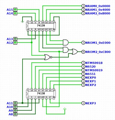
Here's an approach with a few chips that appears to work correctly (though it's certainly not the fastest decode it's only a handful of nanoseconds and should have no issues with a 2MHz clock). Inputs on the left, outputs on the right.

Attachment:
Decode.png
Decode.png [ 72.01 KiB | Viewed 5821 times ]


Half a '139 is used to initially separate the memory space into four 16k blocks (the N before the output names indicates a low-going output, which is almost always what you want for this kind of thing).

The other half of the '139 is enabled by the 0xc000-0xfff output of the first half, and further decodes that section into four blocks of 4k each. The higher two outputs are ANDed together to give the rom at 0xe000-0xffff, easy, but the other ram is a little more complex since you want to enable it for only 6k of its 8k - the remainder of the addressing is for the IO.

When both A11 and A12 are low, we want to enable the IO and disable the rom: a NOR gate gives a high output at that time which is ORed with the ANDed lower two outputs from the '139.

(Or think of it the other way around: the lower two outputs are ANDed to select 0xc000-0xdfff, and that output is later disabled for 0xc000-0xc800)

The block of 0xc000-0xc7fff is decoded into the eight IO selects by the '138, enabled by both 0xc000-0xd000 being active and A11 being low.

Neil


Top
 Profile  
Reply with quote  
PostPosted: Fri Mar 29, 2024 5:33 am 
Offline

Joined: Wed Aug 21, 2019 6:10 pm
Posts: 217
Another way to keep it to two logic gate ICs might be to OR the top 16KB /Select with NOT(A13) to generate a select for the top ROM directly, /ROM2, and with A13 to generate the /IO_ROM1 select for the second half of the 139, breaking the lower IO_ROM1 space between IO and ROM. Now you have a single /IOSelect of the 138 directly from a 139 output, so NOT(/IOSelect) can be ORed with the /IO_ROM1 select to get the /ROM1 select.

The dual 2-4 decoder and the 3-8 decoder, 3 OR's (1 gate free on a quad 2-input OR), 2 NOTs, (4 gates free on a hex inverter, 2 gates free on a quad 2-input NAND).


Top
 Profile  
Reply with quote  
PostPosted: Sun Mar 31, 2024 6:50 pm 
Offline

Joined: Wed Aug 21, 2019 6:10 pm
Posts: 217
Actually, I wonder whether it can be done with three glue logic chips ... a dual 2-4 decoder, a single 3-8 decoder, and a Quad NOR. I hadn't considered this, because the ROM1 select is behind 2 decoder stages and 3 NOR gates, but with a sufficiently fast logic family, and operating at 2MHz, maybe it's workable.

The idea is to use the second half of the 2-4 decoder as a 1-2 decoder.

DECODE1_1A := A14
DECODE1_1B := A15
DECODE1_1Y0 =: /RAM0
DECODE1_1Y1 =: /RAM1
DECODE1_1Y2 =: /RAM2
DECODE1_1Y3 =: /HI_ADDR

/DECODE1_2G := /HI_ADDR
DECODE1_2A := A13
DECODE1_2B := GND
DECODE1_2Y0 =: /ROM1_IO
DECODE1_2Y1 =: /ROM2
DECODE1_2Y2 =: DNC
DECODE1_2Y3 =: DNC

NOR_A1 := A11
NOR_B1 := A12
NOR_Y1 =: DECODE2_G1 =: NOR1_A2 ; IO/ROM

DECODE2_G1 := NOR_Y1 ; IO/ROM
/DECODE2_G2A := /ROM1_IO
/DECODE2_G2B := /ROM1_IO
DECODE2_A := A8
DECODE2_B := A9
DECODE2_C := A10
DECODE2_Y0 =: /IO0
DECODE2_Y1 =: /IO1
DECODE2_Y2 =: /IO2
DECODE2_Y3 =: /IO3
DECODE2_Y4 =: /IO4
DECODE2_Y5 =: /IO5
DECODE2_Y6 =: /IO6
DECODE2_Y7 =: /IO7

NOR_A2 := /NOR_Y1 ; IO/ROM
NOR_B2 := /ROM1_IO
NOR_Y2 =: NOR_A3 ; ROM1

NOR_A3 := NOR_Y2 ; ROM1
NOR_B3 := GND
NOR_Y3 =: /ROM1


Top
 Profile  
Reply with quote  
PostPosted: Sun Mar 31, 2024 7:45 pm 
Offline

Joined: Mon Jan 19, 2004 12:49 pm
Posts: 660
Location: Potsdam, DE
It's that breakdown into 1/4 and 3/4 that complicates matters... :mrgreen:

Neil


Top
 Profile  
Reply with quote  
PostPosted: Sun Mar 31, 2024 8:08 pm 
Offline

Joined: Wed Aug 21, 2019 6:10 pm
Posts: 217
barnacle wrote:
It's that breakdown into 1/4 and 3/4 that complicates matters... :mrgreen:

Neil


Yeah, the 1/4, 3/4 is what attracted my attention to an NOR %00=%1, {%01, %10, %11}=%0 ... if using universal gates to reduce chip count (at the cost of more gate delays), NAND if it is the top quarter, NOR if it is the bottom quarter.


Top
 Profile  
Reply with quote  
Display posts from previous:  Sort by  
Post new topic Reply to topic  [ 7 posts ] 

All times are UTC


Who is online

Users browsing this forum: No registered users and 7 guests


You cannot post new topics in this forum
You cannot reply to topics in this forum
You cannot edit your posts in this forum
You cannot delete your posts in this forum
You cannot post attachments in this forum

Search for:
Jump to: