That pic shows in my phone with the chip, and therefore the text on it, horizontal - so I guess my phone has been lying to me about what image actually look like. Sorry about that.
BigDumbDinosaur wrote:
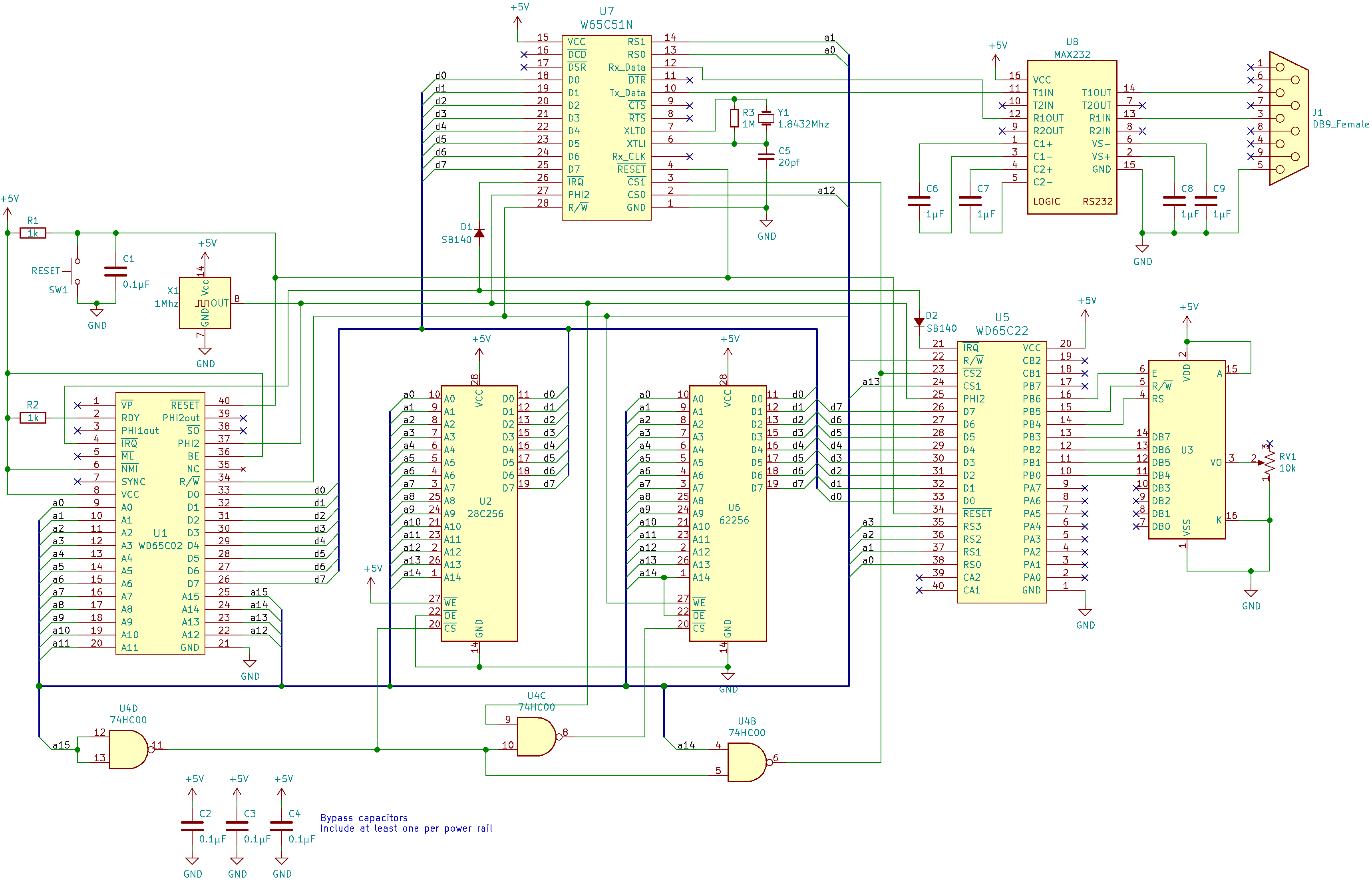
The internal pull-ups are pretty weak, in my opinion, and if a Tx input is to be floated, should be supplemented with a 4.7K resistor to VCC to make the Tx input less noise-sensitive. Being pulled up in this fashion results in the Tx output being in a continuous MARK condition. Despite being unnecessary, there is no harm in having the external pull-up in the circuit for a “live” Tx channel, other than some increased loading on the corresponding UART output.
Ok - I’ll pull it up through a 3.3k “for now” and lay my hands on some 4.7k. I bought a small pile of 3.3k and stopped using the 1ks that came with the kit as the primer advises a 3.3k for everything the kit schematic uses a 1k for. Which means …
BigDumbDinosaur wrote:
For that reason, I recommend that unused Rx channel inputs be pulled up to VCC through no more than 1K of resistance. This will keep the input well above the “no man’s land” input threshold and result in the corresponding Rx output continuously being at logic 0, since the corresponding input will continuously be at SPACE.
… I definitely have a 1k I can use for this right now.
BigDumbDinosaur wrote:
Lastly, my most recent POC units used MLCCs for the charge pump capacitors. I used to use tantalums, but decided to see if the less-expensive MLCCs would work okay...which they do. Pay attention to layout: the charge pump caps should be as physically close to the MAX232 as possible. Also, be sure to bypass the MAX’s VCC with a parallel combination of a 1 µF MLCC and 100 µF low-ESR electrolytic, both caps being in close physical proximity to the MAX232.
I currently have the caps as close as the breadboard will let me but with only a 1 µF on VCC - which is how it is in the circuit in the datasheet I have. I definitely appreciate the advice, thank you!


