6502.org Forum  Projects  Code  Documents  Tools  Forum
It is currently Sat Apr 27, 2024 7:28 pm

All times are UTC


Post new topic Reply to topic  [ 37 posts ]  Go to page Previous  1, 2, 3  Next
Author Message
PostPosted: Fri Jul 07, 2023 8:23 pm 
Offline
User avatar

Joined: Sat Jul 24, 2021 1:37 pm
Posts: 282
AndrewP wrote:
I got so excited here! For my bank zero use case (rather than the general how to detect zero use case) I could use a '573 and a '563 both latching the bank address and saving me that one gate delay and also saving me from reworking the rest of my address decoding.

And then I started looking for inverting latches. And there was no 74LVC563 nor 74LVC533. And I was sad. But then I found a 74ABT533!* :D

And it's not generally stocked with only large quantity orders available on DigiKey. And then I was sad again :(. That's the rollercoaster I put myself on by trying to use all discrete ICs :lol:

*I've found the ABT family to be ridiculously fast - sometimes faster than LVC.


74AC563 propagates in 5.6 typical, where 74LVC573 propagates in 4.3 typical, and 75ABT533 in 4.9 typical (but it has 5V TTL levels). I would argue using an available AC inverting chip is still better than an LVC540.

As you said, these are differences so small they don't really matter that much. Thing is, all the options in this thread have other constraints than raw speed, such as supply voltage, I/O levels, power consumption etc. To design a working board you have to take all of that into consideration, so the choice can't really happen in a vacuum like this. What's the logic behind your /BANK0 signal, is it CMOS, is it running at 5V, etc?

_________________
BB816 Computer YouTube series


Top
 Profile  
Reply with quote  
PostPosted: Fri Jul 07, 2023 11:11 pm 
Offline
User avatar

Joined: Fri Dec 12, 2008 10:40 pm
Posts: 1000
Location: Canada
GARTHWILSON wrote:
AndrewP wrote:
The rising will be pretty quick, but the propagation time to get the output to go from high to low will be really long (ie, slow), because the pull-down resistor has to charge all the capacitance on the diodes and other things connected there, and you have a bad RxC time constant to deal with.


The diodes I mentioned have a capacitance of less than 2pF each. Total will be around 12pF. with R=500 ohms the pd would be < 8ns or so worst case (all 8 charging state).

It was just a thought.

_________________
Bill


Top
 Profile  
Reply with quote  
PostPosted: Sat Jul 08, 2023 3:07 am 
Offline
User avatar

Joined: Fri Aug 30, 2002 1:09 am
Posts: 8428
Location: Southern California
BillO wrote:
GARTHWILSON wrote:
AndrewP wrote:
The rising will be pretty quick, but the propagation time to get the output to go from high to low will be really long (ie, slow), because the pull-down resistor has to charge all the capacitance on the diodes and other things connected there, and you have a bad RxC time constant to deal with.

The diodes I mentioned have a capacitance of less than 2pF each. Total will be around 12pF. with R=500 ohms the pd would be < 8ns or so worst case (all 8 charging state).

8ns would probably be very good.  There are other stray capacitances in the circuit though, ie, that of the input(s) this feeds, possible sockets, traces, etc., and 500Ω is an awfully heavy load, so you'll get nearly 10mA when one or more inputs are high, so then you'll have to consider inductances too...and things could start to get a little messy.  I've used diode logic a lot, but not in anything where I want this kind of speed.

_________________
http://WilsonMinesCo.com/ lots of 6502 resources
The "second front page" is http://wilsonminesco.com/links.html .
What's an additional VIA among friends, anyhow?


Top
 Profile  
Reply with quote  
PostPosted: Sat Jul 08, 2023 12:41 pm 
Offline
User avatar

Joined: Mon Aug 30, 2021 11:52 am
Posts: 251
Location: South Africa
BigDumbDinosaur wrote:
Something to consider is in the realm of bank $00 detection, you only need to decode the number of bits you are actually using. In a 512KB system, that would be three bits.
That is a very good point thanks! Something I just hadn't thought of.

BigDumbDinosaur wrote:
Not to rain on your parade, but the 74ABT533 is a Bi-CMOS device that produces TTL-level outputs. Also, 74F and 74LS produce TTL outputs. These devices’ usefulness is questionable with a WDC MPU or peripheral device.
Ah, this made me realise I've moved the thread out of the range of the newbies sub-forum but not posted enough detail on my setup.

Some important missing information - now that I'm talking about logic families and nanoseconds - is that I run a TTL level board. The only 5V CMOS part I have is the '816. All signals into are up translated using a 74ALVC164245. The data lines, all four interrupts, BE and PHI2. (I treat RDY as an output). Very random story but I managed to find about 600 74ABT245s that were being sold at 20c a chip instead of R20.00 a chip. Buying the lot was not a hard decision. However now I have 600 of the things and I don't know what to do with them so they're getting scattered everywhere I might want to gate or buffer debug signals. They're all playing happily with the LVC chips I usually use.


Top
 Profile  
Reply with quote  
PostPosted: Sat Jul 08, 2023 12:48 pm 
Offline
User avatar

Joined: Mon Aug 30, 2021 11:52 am
Posts: 251
Location: South Africa
I need to bail for the weekend but I've thought of a way of getting the bank address zero testing done within about 1.6ns of PHI2 going high. It's very specific to the 65C02 and the 65C816, not a general test for zero solution.

As a bit of a brain-teaser I thought I'd leave this here and see if anyone else wants to think about how to do that before I post my (hopefully legit) method after I'm back. :D

akohlbecker wrote:
74AC563 propagates in 5.6 typical, where 74LVC573 propagates in 4.3 typical, and 75ABT533 in 4.9 typical (but it has 5V TTL levels). I would argue using an available AC inverting chip is still better than an LVC540.
And this was the post that suggested how I can do it. In a bit of a vague round about way. 8)


Top
 Profile  
Reply with quote  
PostPosted: Sat Jul 08, 2023 12:56 pm 
Offline

Joined: Fri Jul 09, 2021 10:12 pm
Posts: 741
AndrewP wrote:
I need to bail for the weekend but I've thought of a way of getting the bank address zero testing done within about 1.6ns of PHI2 going high. It's very specific to the 65C02 and the 65C816, not a general test for zero solution.

If you only care about the state of this signal during phase 2, and the diode solution has a very fast edge when going low, then you could use a transistor or inverted PHI2 to pull your output high during all of phase 1, so that any slow transition to high is taken care of at the start of phase 1 and cases where all the address bits are momentarily low during phase 1 don't bring it low in the meantime.


Top
 Profile  
Reply with quote  
PostPosted: Sun Jul 09, 2023 10:57 am 
Offline

Joined: Fri Jan 25, 2019 2:29 pm
Posts: 191
Location: Madrid, Spain
I use two chained 74HC688 in the TIMER section of my 74HCT6526 to detect 16-bit zero. Works like a charm.


Top
 Profile  
Reply with quote  
PostPosted: Mon Jul 10, 2023 5:50 am 
Offline
User avatar

Joined: Mon Aug 30, 2021 11:52 am
Posts: 251
Location: South Africa
daniMolina wrote:
I use two chained 74HC688 in the TIMER section of my 74HCT6526 to detect 16-bit zero. Works like a charm.
Back in the spirit of this discussion (before I derailed it into 65816 raw speed bank zero land); a '688 or '521 seems like the best solution because it's fast and is a single IC. This is the answer to the question I asked in my first post, thank you.

However! :lol: ...


Top
 Profile  
Reply with quote  
PostPosted: Mon Jul 10, 2023 6:38 am 
Offline
User avatar

Joined: Mon Aug 30, 2021 11:52 am
Posts: 251
Location: South Africa
... Adrian's post made me stop and ask: "If I can use a '540 to do the inversion before latching the result then why must I wait until PHI2 high before beginning address decoding?"

Let's say I'm doing some combinatorial logic on the Bank and Address lines. And I want to know if the bank address is zero - I can use four triple or gates wired together to detect 8 bit zero (active low). As long as the result is valid and latched before PHI2 goes high then I have practically no propagation delay after PHI2 goes high. The work is already done and latched.

If we assume a I'm using a W65C816S6TQG-14 with VDD at 5V and with a 20Mhz clock.
Attachment:
Address Predecode.png
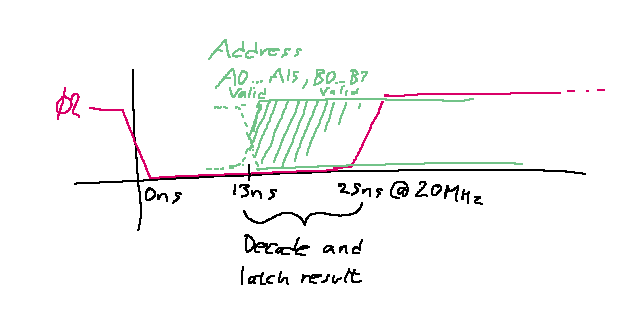
Address Predecode.png [ 10.41 KiB | Viewed 7782 times ]
then I have measured that the address lines become valid after 10 to 11ns. And the bank address lines become valid maybe a bit before 13ns*. This gives around 12ns to do address 'predecoding' and I think in systems with fast clocks that could be quite useful.
Attachment:
Bank is Zero Latch.png
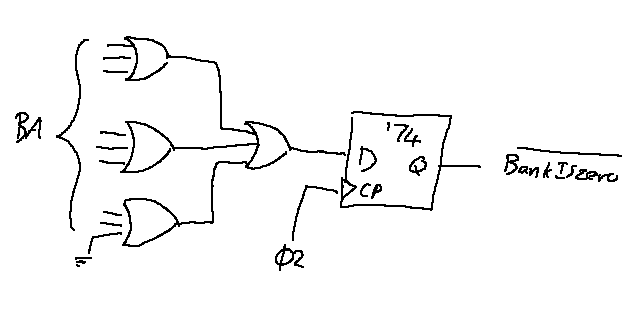
Bank is Zero Latch.png [ 9.53 KiB | Viewed 7782 times ]
If I use four 74LVC1G332s with VCC at 5V and latch their result into a 74LVC1G79 also with VCC at 5V then I get a total propagation delay across that little circuit of 1.6ns + 1.6ns + 1.6ns. Let's just call it 5ns. And that fits easily in the 12ns I had remaining (25 - 13).

Of course after thinking I was really smart to have worked this out I clicked that this is probably the method that 6502 systems have used to deal with address decoding and chip selection since their have been 6502 systems. And probably a lot of 65816 systems too; the WDC suggested circuit just constantly latches the bank address while PHI2 is low. It's only the Bank-Address-is-disappearing restriction in my head that made me think I should only start doing address decoding after PHI2 has gone high and after the '573** has stopped latching.

* Judged by looking at failures at higher clock speeds. The datalines are too chatty for me to actually measure.
** [Edit] Updated '574 to '573. Brainfart or finger trouble but I should have typed '573. Thanks to Garth for spotting that.


Last edited by AndrewP on Mon Jul 10, 2023 8:33 am, edited 3 times in total.

Top
 Profile  
Reply with quote  
PostPosted: Mon Jul 10, 2023 8:15 am 
Offline
User avatar

Joined: Fri Aug 30, 2002 1:09 am
Posts: 8428
Location: Southern California
With all 65xx systems, the entire address, including the bank address on the'816, must be valid and stable for address decoding to begin before Φ2 goes high.  It has always been this way.  This is covered in the first chapter (after the index page) of the 6502 primer, at http://wilsonminesco.com/6502primer/addr_decoding.html .  The circuit WDC publishes in the '816 data sheet uses a '573 for latching the bank address.  The '573 is a transparent latch, so the output follows the input until Φ2 rises, whereupon the value gets locked in to free up the data bus.

_________________
http://WilsonMinesCo.com/ lots of 6502 resources
The "second front page" is http://wilsonminesco.com/links.html .
What's an additional VIA among friends, anyhow?


Top
 Profile  
Reply with quote  
PostPosted: Mon Jul 10, 2023 9:22 am 
Offline
User avatar

Joined: Thu Dec 11, 2008 1:28 pm
Posts: 10793
Location: England
There is something quite important there, but I wouldn't say it exactly that way myself.(*) I hope this isn't mere pedantry - sometimes it makes good pedagogic sense to be less than completely accurate, and sometimes it's also practically sufficient. But pushing an '02 or '816 system to the highest speeds does need an accurate model.

It is true that the 816 uses the databus for two purposes, and so it's necessary to capture the high bits of the address before phi2 rises. It's useful (but not necessary) to use a transparent latch to do that capture, as it gives you more time, and therefore allows the possibility of running faster. And it's a nice idea to do some of the decoding upstream of that latch - maybe allowing for a smaller latch.

Personally I like to distinguish between an edge-sensitive and a level-sensitive capture by referring to the former as a flop or flip-flop and the latter as a latch or a transparent latch.

(*) Some 6502 family peripheral chips capture their chip select inputs on the rising edge of phi2, I think, and for those chips it is necessary to get the decoding done before that. Otherwise, in a simple '02 system, the rising edge of phi2 is merely a convenient timing point. It's the falling edge where work is done, and it's relative to the falling edge that timing constraints apply. In an '816 system, the rising edge of phi2 does serve a timing purpose. Systems which use the first half of the cycle for other purposes, such as video access to RAM, also need to care.


Top
 Profile  
Reply with quote  
PostPosted: Mon Jul 10, 2023 10:02 am 
Offline

Joined: Fri Jul 09, 2021 10:12 pm
Posts: 741
I was also going to ask if anybody knows of 6502 instructions that have cycles in which the address bus changes later than usual during phase 1 - or is the mechanism for getting the address onto the bus common to all cycles. E.g. when there's a carry to compute maybe it could change again later in phase 1 - but I think in those cases it always just adds an extra cycle to the instruction?

The datasheet specifies a minimum time to wait (maximum time it could take to be ready) but if you're driving for higher clock speeds than the official ratings then I imagine that is an area where you need to take more liberties.


Top
 Profile  
Reply with quote  
PostPosted: Mon Jul 10, 2023 11:15 am 
Offline
User avatar

Joined: Thu Dec 11, 2008 1:28 pm
Posts: 10793
Location: England
I'm tempted to say the delay (in nanoseconds) will be the same for all instructions. A trace with a suitable scope should answer the question. JMP might be an interesting case because the MSB of the address comes directly from the previous cycle's read on the databus - and that data could arrive quite late. Then again, there is a setup time constraint, so it isn't supposed to be too late.


Top
 Profile  
Reply with quote  
PostPosted: Mon Jul 10, 2023 7:01 pm 
Offline
User avatar

Joined: Fri Aug 30, 2002 1:09 am
Posts: 8428
Location: Southern California
BigEd wrote:
(*) Some 6502 family peripheral chips capture their chip select inputs on the rising edge of phi2, I think, and for those chips it is necessary to get the decoding done before that. Otherwise, in a simple '02 system, the rising edge of phi2 is merely a convenient timing point. It's the falling edge where work is done, and it's relative to the falling edge that timing constraints apply. In an '816 system, the rising edge of phi2 does serve a timing purpose. Systems which use the first half of the cycle for other purposes, such as video access to RAM, also need to care.

Even for some other non-65xx parts, I suspect there could be some danger if a write is started while the address could still be changing.  It may be safe for some, while for others it could cause problems that may be very difficult to trace down.  The solution then would be to either delay the WE\, or just make sure all the address and select lines are valid and stable well ahead of the rise of phase 2.

_________________
http://WilsonMinesCo.com/ lots of 6502 resources
The "second front page" is http://wilsonminesco.com/links.html .
What's an additional VIA among friends, anyhow?


Top
 Profile  
Reply with quote  
PostPosted: Mon Jul 10, 2023 7:10 pm 
Offline
User avatar

Joined: Thu Dec 11, 2008 1:28 pm
Posts: 10793
Location: England
Good point, write should be gated to some time where the address decoding is stable. Phi2 is convenient for that - but only convenient, not the actual definition of the right window!


Top
 Profile  
Reply with quote  
Display posts from previous:  Sort by  
Post new topic Reply to topic  [ 37 posts ]  Go to page Previous  1, 2, 3  Next

All times are UTC


Who is online

Users browsing this forum: No registered users and 7 guests


You cannot post new topics in this forum
You cannot reply to topics in this forum
You cannot edit your posts in this forum
You cannot delete your posts in this forum
You cannot post attachments in this forum

Search for:
Jump to: