My apologies from the start for a verbose post. Some of this is just how to read your scope screen, or at least what I see and think is/isn't important when I look at your scope screen.
adrianhudson wrote:
Here are some recent shots from my (ahem) oscilloscope:
Don't knock your oscilloscope - it likely can help solve the problem. One thing I note is that your scope is 2 channel, but you are only showing 1-channel shots. Because everything is timed to the clock, having the clock on one channel (and triggering off that channel) and using the second channel to probe around (with both channels on the screen) can help us see timing issues. The data lines, in particular, have times when no-one is driving them and they can float (which likely explains some of the curved sections of your data lines; with pullups they will trend in the upward direction when not driven by an output).
Let's go through your scope shots and I will tell you what I see in each one, and then recommend some useful places to look based on what we think the issues might be. I am not an expert on the 6502, but I use oscilloscopes all the time for work (both nice/expensive ones and cheap ones - sometimes the cheap ones are easier to use).
adrianhudson wrote:
This is phi2 at the 'C02 pin37 with the probe GND lead removed and a GND spring to the oscillator can (its that close)
Attachment:
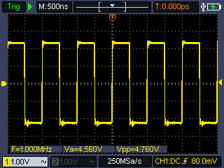 at phi2 in pin to can with probe spring gnd.png [ 5.36 KiB | Viewed 3433 times ]
Thank you for clearly describing how you grounded your probe. I see a reasonably good looking square wave at 1MHz. I can see that you have properly adjusted the compensation on your probes (assuming you are using the 10X setting, which you should prefer when possible). I do note that GND (indicated by the thicker yellow arrow at the left of the screen) is in the middle of this waveform, but then I also notice that channel 1 is in AC mode by looking in the lower left and seeing the sine wave next to channel 1. AC mode subtracts the DC offset and puts the "average" voltage at 0V on the screen. We will generally prefer DC mode for all waveforms for digital logic work except for a few special cases. I do see a little wiggle at the bottom of the waveform, just after the falling edge, that might be something interesting (especially if it shows up in other places at larger amplitudes), but it is unconcerning at the amplitude shown. This is a perfectly good clock here, but it's right at the oscillator output - you will want to see what it looks like in other places (using the ground of the chip you are probing it on).
adrianhudson wrote:
This is A0 at the CPU. You can see the clock noise
Attachment:
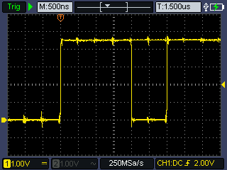 A0 at CPU.png [ 5.17 KiB | Viewed 3433 times ]
This looks like a very good A0 signal. I don't see anything that concerns me here. Your ground is properly connected (looking at the large yellow arrow at the left side of the screen). I do note that your scope is showing multiple traces on top of each other (looking at the right side where it appears the signal is high and low at the same time). This is OK as long as you know your scope does this. You might have trace persistence turned on, but a glance in the user's manual for your scope does not show a way to turn it on/off. Because we are potentially looking for "glitches", we actually prefer this mode of looking at things because it will show normal looking traces AND the glitchy one if it happens while the scope is looking.
adrianhudson wrote:
Here is +5V at the oscillator pin
Attachment:
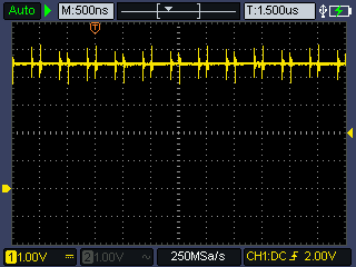 5V at osc can.png [ 4.92 KiB | Viewed 3433 times ]
Normally I might be concerned at the ringing spikes that are not 500ns apart (we expect small ringing at both rising and falling clock edges, but not when the clock is steady high or steady low), however we know (from your previous scope shot) that your scope shows multiple traces overlapped and I see your trigger (the smaller yellow arrow on the right) isn't at a useful level here. Your trigger is set to 2V rising edge (as noted in the bottom right corner) however this trace has no portion that crosses 2 V in either direction, so the scope is auto-triggering (as noted in the upper left hand corner). This means the scope just picks a starting time (not synchronized with the signal) and draws the trace. Because your scope shows multiple traces of the signal on the screen, we get what appears to be 2 traces, both with the expected ringing at 1MHz rate, but they are not properly overlaid on top of each other. To fix this, move the trigger point up until it is in the trace. I'd move it up to the lowest point (below the 5V level) where it reliably triggers (as noted by "Trig" appearing in the upper left corner of the screen). Having the clock on one channel and triggering off it would also fix this issue.
It's worth noting that the amplitude of the ringing is about +/- 0.5V. That's not a terrible or unexpected level here, but it is worth looking in other places as well. Because they are only one pixel wide, I would zoom in to investigate them, but they should be fine here. It's worth looking at 5V of all the chips, but make sure you are using the ground for that particular chip so you get an idea of what the chip actually sees for power.
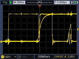
adrianhudson wrote:
I have the pullup resistors still attached on the data lines, so I disconnected the resistor on D0 and here is a trace of D0 at the RAM chip pin
Attachment:
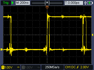 D0 at RAM pull disconnected.png [ 5.45 KiB | Viewed 3433 times ]
This scope shot is interesting. We have multiple overlapping traces of this signal again, which makes things a bit confusing. The only place where the signals really should be overlapping is at the trigger point (noted by the orange T at the top of the screen) and all traces should be a rising edge crossing 2V (as per your settings in the lower right corner). The interesting part here is that D0 is being driven high (rising edge at the trigger point in the middle of the screen) and the immediately driven low about 50ns later on at least one trace. That doesn't look like a pullup driving it high (it's too fast of a rise) and it doesn't look like it is floating - it looks like it is being actively driven high and then low. This might be related to your issue and it is worth investigating.
The other overlapping areas are inconclusive because we can't tell which trace is high or low before and after the transition. Because there is that small gap at the bottom, just after the trigger point, I can tell that there is at least 1 trace that went high and then very quickly went low. As noted by others, the older micros might be too slow to even notice but the newer WDC parts may see that and sample the data during the glitch. Having everything synchronized to the clock using a second trace would likely make this much clearer and help determine if it's a problem or not. If the falling edge is during (or even very close) to that kind of glitch, it might be your problem.
adrianhudson wrote:
Here is D1 (with its pullup attached) at the RAM chip pin
Attachment:
 D1 at RAM pullup.png [ 5.96 KiB | Viewed 3433 times ]
Clock noise is everywhere and what are those curved - really slow rise lines on D1 (with pullup) (they are also on D2-7)?
When using pullups, the "shark fin" sections are totally normal. That's the resistor "charging" the capacitance of the bus and is a standard Resistor-Capacitor charging curve. The resistors are there to help finish pulling up for chips that can only pull part-way up but not quite high enough (one of the potential issues were were looking for based on the discussion so far). The data only needs to be valid at the falling edge of the clock (so falling edge would be good for triggering on the clock on a second channel here), so it's technically OK to be in the middle as long as it's not on a clock edge. I don't really see any waveforms that look like the data line isn't getting high enough, and the sharkfins shown look like times the bus simply isn't driven by any chip. The sharkfin in the middle is an entire half-cycle that the bus was not driven. The sharkfin on the right is a little more interesting. The bus was undriven for about 100ns before someone decided it should be low and drove it low (most likely propagation delay in chip select and inside the memory). The little double sharkfin drawn in the same place is a little weird, though.
adrianhudson wrote:
Sorry about the really rubbish scope folks - I know the John Ruskin quote (
https://www.nthong.co.uk/ruskin.htm ) but I regularly ignore it, much to my disadvantage!
Your scope is fine and should be plenty good enough to locate and solve this problem.
Recommended setups:
Have both channels on the screen. Trigger on the rising edge of the /CS line of RAM (which will be the end of the RAM read or write cycle, so look at the other lines just
before the trigger point) and use the other channel to look at /WE, /OE, and D0 (I'm picking this one because you've indicated D0 is different when it isn't working - when you said a failed memory test showed the "previous" count value) at the RAM chip and also at the 6502. If you make a test program that only reads or only writes to ram, then you will know that all RAM accesses are reads (or writes) when those programs are running and the chip select on the RAM is active (low).
Using /CS of the RAM, rather than the system clock, will let us see only the times your micro is talking to the RAM. It's not clear in the current waveforms if we are seeing the RAM or the ROM (putting the opcodes of the program on the bus) or the micro itself when the data bus is being driven. It would be nice to find an explanation for the approx 50ns wide glitch, or even to verify that it is real. This setup will also let you measure the output voltage of the RAM, specifically, as only the RAM should be driving the bus shortly after it is selected (/CS has gone low) and its outputs are turned on (/OE is also low). Writing a program that only reads from RAM (could be the same location over and over) would help.
You may also want to investigate the other /CS lines on other chips to make sure they AREN'T active (low) when the RAM /CS line is active (low).
If that isn't showing anything interesting, trigger on the falling edge of the clock (because this is when the data will be transferred from one chip to another, but note that not all falling edges have data transfer) and look at the data lines to see if you can reproduce that glitch. If so, it would be good to know if it's only on one data line, or multiple. The data should be valid and stable during the falling edge of the clock and ideally for a little bit of time (eg. 10ns) before and after. Older parts will need a longer setup time (eg. steady BEFORE the falling edge of the clock). Your setup should provide hundreds of ns of setup time. Running at 1MHz is
supposed to be rather easy.


