6502.org Forum  Projects  Code  Documents  Tools  Forum
It is currently Thu May 02, 2024 7:47 pm

All times are UTC


Post new topic Reply to topic  [ 54 posts ]  Go to page Previous  1, 2, 3, 4  Next
Author Message
PostPosted: Sun Feb 27, 2022 10:18 am 
Offline
User avatar

Joined: Thu May 28, 2009 9:46 pm
Posts: 8169
Location: Midwestern USA
akohlbecker wrote:
Never said anything about not qualifying them with the clock also :-) Here is my circuit simulation for read/write pulses (with VA here being VDA OR VPA).

Attachment:
Screenshot 2022-02-27 at 08.39.03.png
I still fail to see where that is useful.

In some cases, failure to qualify addresses with VDA may result in a location being touched during a so-called dead cycle. If that location is a chip register, it being touched may cause the device to behave in an undefined way. It has to do with the fact that some addressing modes result in a partially-formed address being asserted before the true address is emitted.

The purpose of VDA and VPA is to qualify addressing, not read/write operations. In a properly-designed 65C816 system, the glue logic will generate a chip select during Ø2 low, since that is when the address bus becomes valid. However, not all bus cycles generate a usable address. That's why VDA and VPA exist.

_________________
x86?  We ain't got no x86.  We don't NEED no stinking x86!


Top
 Profile  
Reply with quote  
PostPosted: Sun Feb 27, 2022 1:55 pm 
Offline
User avatar

Joined: Fri Dec 11, 2009 3:50 pm
Posts: 3350
Location: Ontario, Canada
For purposes of discussion, let's consider (A) and (B), below. (A) is a widely used snippet familiar to pretty well everyone, and (B) is somewhat similar to the excerpt Adrien posted.

Attachment:
using VDA to qualify RD#.png
using VDA to qualify RD#.png [ 2.85 KiB | Viewed 1034 times ]


BigDumbDinosaur wrote:
In some cases, failure to qualify addresses with VDA may result in a location being touched during a so-called dead cycle. If that location is a chip register, it being touched may cause the device to behave in an undefined way.
Yes, exactly. Users of the original (ie, NMOS) 6502 occasionally get bitten by this, although it is fairly rare. The 6502 has no VDA output. Luckily, 6502 folk are able to solve the problem by being careful in regard to certain programming practices, such as indexed addressing of an I/O device and using Read-Modify-Write instructions on an I/O device.

The same solution is available to '816 users, and therefore it's not "strictly necessary" to use VDA. :!: But using VDA does relieve you of concern about "breaking the rules," and some of us may value that advantage quite a lot. YMMV.

Something worth noting: it's fairly common for I/O devices to include registers (such as the 6522's Interrupt Flag Register) which'll be adversely affected by the spurious read that occurs during a "dead" cycle. (Dead cycles are always reads, never writes.) But as a rule, memory devices simply don't care about a spurious read -- it won't cause the least bit of trouble. The only exceptions would involve wonky stuff like the "knock sequence" used to unlock certain EEPROMs and/or Flash memory chips. (And besides, the potential problem can be sidestepped by following the rules.)

Since only the wonkiest memory chips may benefit from protection against dead cycles, we can usually satisfy ourselves by only protecting I/O... and that's what (B) does. In other words, use RD# and WR# from (B) to drive your I/O devices.

Of course, I/O chips from the 65xx family don't have RD# and WR# inputs. But most (all?) of them have two Chip Select inputs, one active-high and one active-low. If the active-high CS is otherwise unused then the 65xx I/O device(s) in your design can be protected very easily indeed. Simply connect the active-high CS to VDA. :)

-- Jeff

ps- there's a carefully researched list of dead-cycle behaviors here. This includes the 65C02, which has its own unique remedy for the dead cycle issue.

_________________
In 1988 my 65C02 got six new registers and 44 new full-speed instructions!
https://laughtonelectronics.com/Arcana/ ... mmary.html


Top
 Profile  
Reply with quote  
PostPosted: Sun Feb 27, 2022 5:11 pm 
Offline
User avatar

Joined: Fri Dec 11, 2009 3:50 pm
Posts: 3350
Location: Ontario, Canada
A footnote. Some '816 designs use an OR gate so that both VDA and VPA play a role in dead cycle protection. But there are pros and cons, and their relative weight will, as always, depend on prevailing circumstances and priorities. Most often the balance will favor ignoring VPA.

If you want your design to include dead cycle protection you can, as shown in the preceding post, inject a signal into the logic that generates RD# and WR#. In this post I'll show how a signal can be injected into the address decode logic instead. Circuits (i) and (ii) inject the signal at two different points. And circuit (ii) allows VPA to be ignored.
Attachment:
VDA injection points.png
VDA injection points.png [ 23.29 KiB | Viewed 1021 times ]

Obviously circuit (ii) is faster and requires less logic. That said, I suppose situations may exist in which (i) would be a "win." Maybe your level-two decoder doesn't have an extra Enable input that's available, and you're unwilling to rework the circuit. Or maybe you feel memory, too, ought to be protected (although that's virtually always unnecessary, as noted in the previous post). In that case the OR gate and its speed hit may be a price worth paying.

But clearly, VDA alone can be sufficient to 100% protect I/O devices from the spurious read associated with a dead cycle. To anyone contemplating a new design, I suggest you begin with the default assumption that VPA will have no role. Beginning with the opposite assumption can, if you're not careful, lock you into a compromise whose pros and cons aren't the best fit for your needs.

(And a reminder: 65xx I/O devices whose active-high CS is unused can be protected simply by connecting that CS to VDA.)

-- Jeff

_________________
In 1988 my 65C02 got six new registers and 44 new full-speed instructions!
https://laughtonelectronics.com/Arcana/ ... mmary.html


Top
 Profile  
Reply with quote  
PostPosted: Sun Feb 27, 2022 6:39 pm 
Offline
User avatar

Joined: Thu Dec 11, 2008 1:28 pm
Posts: 10793
Location: England
Thanks Jeff, very clear as always!


Top
 Profile  
Reply with quote  
PostPosted: Sun Feb 27, 2022 8:23 pm 
Offline

Joined: Sat Feb 19, 2022 2:18 am
Posts: 47
To reduce the number of variables, I removed the RAM and GAL. I am decoding for the ROM enable with A15#. I have changed back to the HC family of ICs for the '573, '245, and '00. I have also added bodge wire to the back of the PCB for all VCC and GND connections for the ICs being used as part of the core 65816.

So far, results are the same. If I keep the ROM CS# connected to GND, reading ROM seems to be fine. If I try to drive the ROM CS# off A15#, ROM reads are not working.

I have attached the current schematic. I uploaded a video showing what I'm seeing.

Next, I will incorporate VDA/VPA into the simple decode logic.


Attachments:
File comment: Latest schematic
Schem 20220227.png
Schem 20220227.png [ 632.48 KiB | Viewed 1001 times ]
File comment: PCB update
bodge lg.jpg
bodge lg.jpg [ 492.79 KiB | Viewed 1001 times ]
Top
 Profile  
Reply with quote  
PostPosted: Sun Feb 27, 2022 10:18 pm 
Offline
User avatar

Joined: Sat Jul 24, 2021 1:37 pm
Posts: 282
GARTHWILSON wrote:
Quote:
BigDumbDinosaur wrote:
No pullup resistor is required on RWB, as that output is driven in both directions—it's not an open-collector output.[/color]

It is useful if you use Bus Enable as this pin is tri-stated, but not required.

If it's tri-stated, wouldn't it be so something else can drive it? I keep looking over the topic, thinking there's something I'm missing; but in rehsd's schematic, BE's only connection is a pull-up. Otherwise, how fast do you want it? Pull-ups tend to not be useful at the higher 65xx speeds if you want fractional-cycle timing. Consider a line with 30pF total, including the ICs it's connected to, IC sockets, capacitance in the board, etc., and a pull-up of 10K which I'm seeing on plasmo's .pdf of rehsd's schematic. That makes for a time constant of 330ns. (Time constant is the length of time needed to achieve (1-1/e)*total_voltage_swing, or about 63% of the voltage swing. So for 5V CMOS it would be the time required to go from 0V to 3.16V.) You may need more logic to make sure its input swings as fast as you want it to.


On a development board, you might want to have an input for BE you can hook a jumper to, just to try it out or experiment with a circuit. In that case, the pull-up on RWB ensures a defined state of the pin. As with most things, it depends on your project goals: some folks here are building optimized production-like boards with a well defined use case. Myself, I'm building something I can play with and learn and I want all combinations of inputs to have defined behavior. It looks like rehsd's board is also more on the experimental side

Great point on the time constant though! Agreed that for this pin to work fast enough you'd need logic driving it.

BigDumbDinosaur wrote:
akohlbecker wrote:
Never said anything about not qualifying them with the clock also :-) Here is my circuit simulation for read/write pulses (with VA here being VDA OR VPA).

Attachment:
The attachment Screenshot 2022-02-27 at 08.39.03.png is no longer available
I still fail to see where that is useful.

In some cases, failure to qualify addresses with VDA may result in a location being touched during a so-called dead cycle. If that location is a chip register, it being touched may cause the device to behave in an undefined way. It has to do with the fact that some addressing modes result in a partially-formed address being asserted before the true address is emitted.

The purpose of VDA and VPA is to qualify addressing, not read/write operations. In a properly-designed 65C816 system, the glue logic will generate a chip select during Ø2 low, since that is when the address bus becomes valid. However, not all bus cycles generate a usable address. That's why VDA and VPA exist.


The use case where this is useful is DMA. The address decoding is just a static mapping from portions of memory to a hardware device, but if you introduce signals coming from the CPU side into your decoding, how will the DMA device be able to access memory? it would need to generate VDA/VPA itself. However, these signals can't be tri-stated on the CPU side.

If you instead make the RD/WR pulses depend on VDA/VPA, then the address decoding is static, and any address put on the bus by another device generates the correct chip selects. If you also make RD/WR tri-state via Bus Enable on the CPU side, then the DMA device can generate its own RD/WR signals, and work at any frequency, totally independent from the CPU. The same DMA device could then theoretically also work on any CPU because it doesn't have to know about 65C816 specific signals. It is just a better separation of concerns IMO.

Again, this all depends on what you're building and what your goals are. Most likely sending VDA into a '138 leads to faster logic, if your goal is speed that's great.

Dr Jefyll wrote:
A footnote.


Great points all around, thanks Jeff!

rehsd wrote:
To reduce the number of variables, I removed the RAM and GAL. I am decoding for the ROM enable with A15#. I have changed back to the HC family of ICs for the '573, '245, and '00. I have also added bodge wire to the back of the PCB for all VCC and GND connections for the ICs being used as part of the core 65816.

So far, results are the same. If I keep the ROM CS# connected to GND, reading ROM seems to be fine. If I try to drive the ROM CS# off A15#, ROM reads are not working.

I have attached the current schematic. I uploaded a video showing what I'm seeing.

Next, I will incorporate VDA/VPA into the simple decode logic.


Forget about VDA/VPA for now, if you can't get your ROM to output data you have bigger problems :-)

Attachment:
Screenshot 2022-02-27 at 23.10.41.png
Screenshot 2022-02-27 at 23.10.41.png [ 1.62 MiB | Viewed 984 times ]


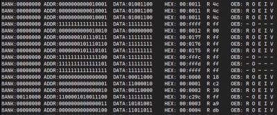
This is an unrelated issue, but your reset vector is not set up properly. Here, the CPU reads from 0xFFFC and 0xFFFD, which both return 0xFF. Then it jumps to 0xFFFF, where it against reads 0xFF. That's a SUB long,X instruction, so it reads the next 3 bytes as data (0x0000, 0x0001, 0x0002 which all return various values). Then it reads 0x30C29C (so at least this means your bank address latching is working, since this is outside of bank 0 :-) )
Then it continues at 0x0003 with 0xA9, which is your LDA #$DB

You probably want 0xFFFC,D to point to the start of ROM at address 0x8000. In this case, the CPU is skipping over your CLC and REP #%00110000 (the CLC makes me think you're also missing an XCE in there to enable native mode?)

I have looked at your updated schematic, and I have not found any problems. How confident are you in your routing? Did you run an ERC check on your design?

_________________
BB816 Computer YouTube series


Top
 Profile  
Reply with quote  
PostPosted: Sun Feb 27, 2022 10:26 pm 
Offline
User avatar

Joined: Sat Jul 24, 2021 1:37 pm
Posts: 282
Actually, isn't that your problem?? :idea:

Attachment:
Screenshot 2022-02-27 at 23.23.01.png
Screenshot 2022-02-27 at 23.23.01.png [ 1.31 MiB | Viewed 984 times ]


This is the first case with the ROM being driven by A15. If your ROM does indeed contain 0xFF at 0xFFFC and 0xFFFD, then this behaviour is expected, the CPU jumps to 0xFFFF then wraps around to 0x0000 while processing the SUB long,X instruction. Then it reads 0x00 from your RAM, which is BRK, and you see it process the interrupt by saving data onto the stack (the three following writes).

My guess is your ROM is working, but you're missing a reset vector :mrgreen:

_________________
BB816 Computer YouTube series


Top
 Profile  
Reply with quote  
PostPosted: Sun Feb 27, 2022 11:54 pm 
Offline

Joined: Sat Feb 19, 2022 2:18 am
Posts: 47
akohlbecker wrote:
Actually, isn't that your problem?? :idea:

Attachment:
Screenshot 2022-02-27 at 23.23.01.png


This is the first case with the ROM being driven by A15. If your ROM does indeed contain 0xFF at 0xFFFC and 0xFFFD, then this behaviour is expected, the CPU jumps to 0xFFFF then wraps around to 0x0000 while processing the SUB long,X instruction. Then it reads 0x00 from your RAM, which is BRK, and you see it process the interrupt by saving data onto the stack (the three following writes).

My guess is your ROM is working, but you're missing a reset vector :mrgreen:

I will be very excited if this is just an assembly coding issue (which would not at all surprise me!). Looking into it...


Top
 Profile  
Reply with quote  
PostPosted: Mon Feb 28, 2022 12:13 am 
Offline

Joined: Sat Feb 19, 2022 2:18 am
Posts: 47
Here is the assembly that I am using:
Code:
.org $0000
reset:
    clc
    rep #$30            ;set 16-bit mode

    lda #%11011011      ;$DB

    sta $1000
    sta $2000
    lda $1000
    lda $2000

    jmp reset

I see that I am missing the xce call after the clc (so I'm still in emulation mode). My understanding is that in emulation mode, 00FFFC,FD is used for RESET. In native mode, there is no RESET vector. So, my first question... Do I always need a RESET vector since the processor always starts in emulation mode? And then I can switch to native mode with clc, xce once it's running in the reset vector? Looking at my code above, I probably need to change the .org before the reset: to $8000 and add a .org to get me to the reset vector. Something like this:
Code:
    .org $fffc
    .word reset

Does that sound right?


Top
 Profile  
Reply with quote  
PostPosted: Mon Feb 28, 2022 1:22 am 
Offline

Joined: Sat Feb 19, 2022 2:18 am
Posts: 47
I updated my assembly to that in the attached image. I filled the remainder of the flash ROM with 'AA' so I could see if it was pulling something in the remainder of the ROM (versus 'FF'). I can see in the debug output that it's pulling 'AAAA' from the ROM for the reset instead of '8000', so now I need to track that down. I have verified continuity for all address lines to the flash ROM. If I'm getting 'AA', it must be pulling it from an address greater than $FFFF. My first thought is that A16-18 must be coming through with a bit set to '1' for it to get to the 'AA' values. (I'm just thinking out loud at this point and need to noodle more on this.) Or my references to addressing are wrong somewhere. More to come...


Attachments:
File comment: Debug output
output.png
output.png [ 18.89 KiB | Viewed 967 times ]
File comment: Reset vector in ROM
ROM.png
ROM.png [ 3.53 KiB | Viewed 967 times ]
File comment: Source assembly
assembly.png
assembly.png [ 24.53 KiB | Viewed 967 times ]
Top
 Profile  
Reply with quote  
PostPosted: Mon Feb 28, 2022 1:27 am 
Offline

Joined: Fri Dec 21, 2018 1:05 am
Posts: 1076
Location: Albuquerque NM USA
65816 definitely needs reset vector at $FFFC and $FFFD, so the ".org $fffc" and ".word reset" are required.

Looking at the image of your pc board, I see on the top side there is a trace running very close to pin 9,10,11,12,13,14 of a 14-pin DIP next to 74AHC74. Can't read the part number but is it 74HC00, the one you are having problem with? Trace is actually shorted to the pins on the image, but is that just an illusion?
Bill


Top
 Profile  
Reply with quote  
PostPosted: Mon Feb 28, 2022 1:59 am 
Offline

Joined: Sat Feb 19, 2022 2:18 am
Posts: 47
plasmo wrote:
Looking at the image of your pc board, I see on the top side there is a trace running very close to pin 9,10,11,12,13,14 of a 14-pin DIP next to 74AHC74. Can't read the part number but is it 74HC00, the one you are having problem with? Trace is actually shorted to the pins on the image, but is that just an illusion?
Bill

Hi, Bill. I'm trying to determine where you're looking. Any chance you could post a pic with it circled? My 74AHC74 is on the small clock board stuck to the top of the main PCB.


Top
 Profile  
Reply with quote  
PostPosted: Mon Feb 28, 2022 2:19 am 
Offline

Joined: Fri Dec 21, 2018 1:05 am
Posts: 1076
Location: Albuquerque NM USA
It is the 14 DIP above VIA1 and below 65816 (not directly below, but low right of 65816). The image I'm looking at is marked "TOP" of this post:
viewtopic.php?f=12&t=7032&start=15#p91004
Bill


Top
 Profile  
Reply with quote  
PostPosted: Mon Feb 28, 2022 2:41 am 
Offline

Joined: Sat Feb 19, 2022 2:18 am
Posts: 47
I think I see what you're looking at. Yes, it's just an illusion. I quickly checked the board. I am not using that IC location at the moment, but it was good to check. Those general IC locations only have VCC and GND connected (with pin headers for actual connection to the rest of the circuit).

I missed Adrien's question earlier about ERC. Yes, this was checked with EasyEDA.


Attachments:
pcb check3.jpg
pcb check3.jpg [ 2.03 MiB | Viewed 958 times ]
pcb check2.jpg
pcb check2.jpg [ 2.52 MiB | Viewed 958 times ]
pcb check1.png
pcb check1.png [ 476.68 KiB | Viewed 958 times ]
Top
 Profile  
Reply with quote  
PostPosted: Mon Feb 28, 2022 4:25 am 
Offline

Joined: Sat Feb 19, 2022 2:18 am
Posts: 47
akohlbecker wrote:
Actually, isn't that your problem?? :idea:

Attachment:
The attachment Screenshot 2022-02-27 at 23.23.01.png is no longer available


This is the first case with the ROM being driven by A15. If your ROM does indeed contain 0xFF at 0xFFFC and 0xFFFD, then this behaviour is expected, the CPU jumps to 0xFFFF then wraps around to 0x0000 while processing the SUB long,X instruction. Then it reads 0x00 from your RAM, which is BRK, and you see it process the interrupt by saving data onto the stack (the three following writes).

My guess is your ROM is working, but you're missing a reset vector :mrgreen:


:D :D :D
I have it working! Great catch, Adrien! My assembly coding was at fault. And now I have a list of other nice improvements to make, based on all the great ideas shared in this thread. I have attached the code I'm using, along with the results of a successful write to, and read from, RAM. Because I'm wasting the first 32K of the ROM (addresses are used by RAM), I have to make sure my ROM starts at $8000. Just using a .org with $8000 ended up with the assembler writing it to $0000. I had to write some junk at $0000 and then the .org $8000 kept my assembly in the proper location.

Thank you, Adrien, and everyone, for all the help!! This community is awesome!


Attachments:
ROM RAM working - logging.png
ROM RAM working - logging.png [ 96.37 KiB | Viewed 948 times ]
ROM RAM working - assembly.png
ROM RAM working - assembly.png [ 172.83 KiB | Viewed 948 times ]
Top
 Profile  
Reply with quote  
Display posts from previous:  Sort by  
Post new topic Reply to topic  [ 54 posts ]  Go to page Previous  1, 2, 3, 4  Next

All times are UTC


Who is online

Users browsing this forum: gluesniffing and 3 guests


You cannot post new topics in this forum
You cannot reply to topics in this forum
You cannot edit your posts in this forum
You cannot delete your posts in this forum
You cannot post attachments in this forum

Search for:
Jump to: