BigDumbDinosaur wrote:
Every device has a 0.1 uF bypass capacitor. Also, one is placed at the power connector to keep circuit noise from sneaking out the back door and causing RFI. Another is placed by a header that can be configured to power an external terminal adapter. That's why you see so many of them. Bypass capacitors are like money: no such thing as "too much."

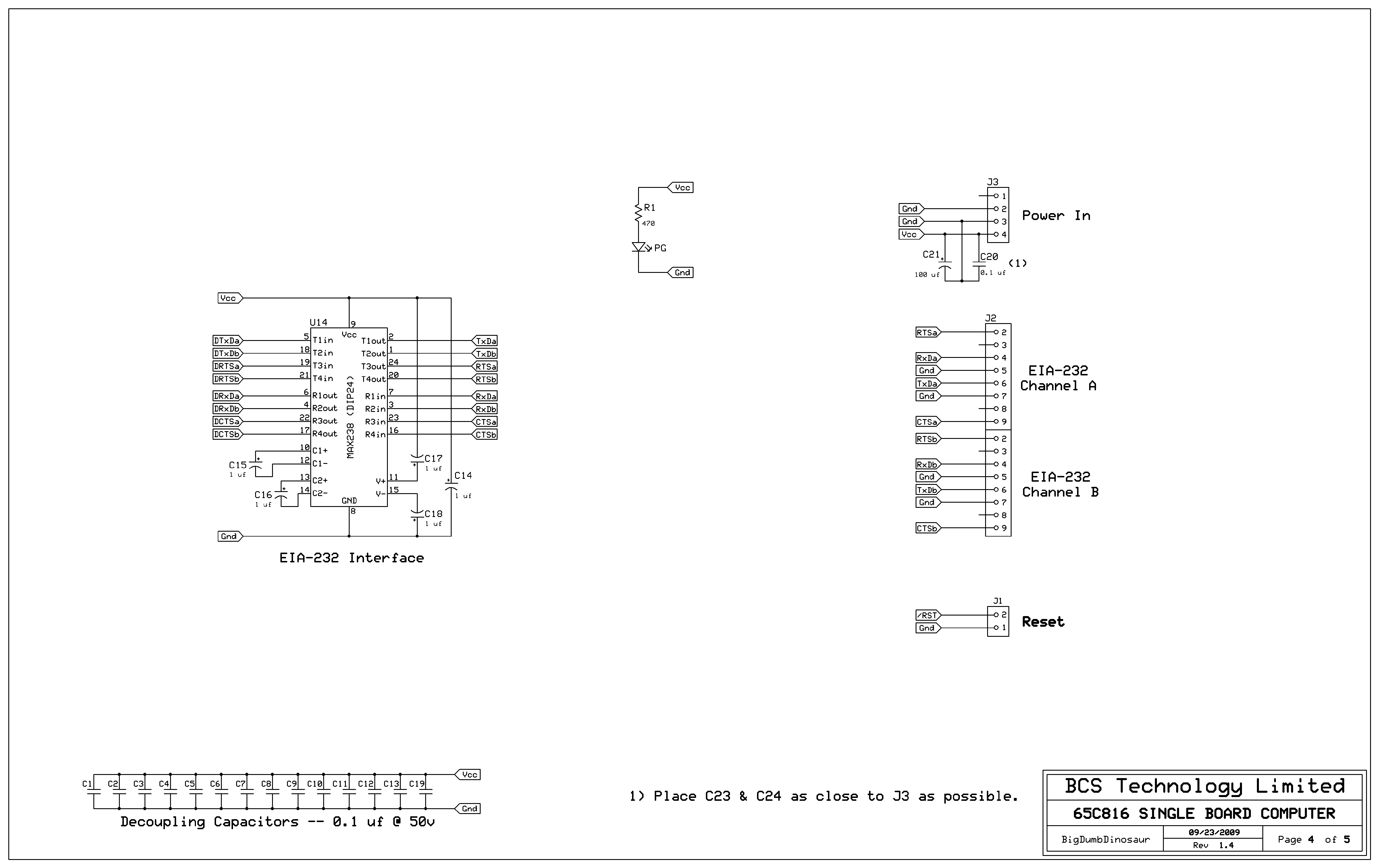
So let me understand your schematic correctly then:
http://sbc.bcstechnology.net/images/sbc_v1_page04.gifAt the bottom left corner, you have a BUNCH of capacitors all in a row. What you are implying is that there is one capacitor there for each component, and that it's placed at the VCC side of that component? You are not using some 20x capacitor array network or something?
BigDumbDinosaur wrote:
For a first effort, I'd suggest you do it in two-layers to gain design skills with component placement and circuit routing.
I've been thinking of a 2-layer design for a while. I don't know trace sizes very well, I know they are dependent on amps and all that, but there are numerous factors at play. My logic lines always seem too small, and my power lines always seem too big. With that in mind, what if I were to make a 2-layer board, but knowing that I will connect all VCC and GND pins with wires on the bottom. Like how you had to perform 'surgery' on your board, but knowing that I will be doing that going into it. Would that help with sizing? With something like that, could I more easily fit some decoupling capacitors in there? It's probably a dumb idea, but I think I need someone to tell me that before I really believe it.
BigDumbDinosaur wrote:
The device's VCC pin should be connected by a short and relatively wide trace to the VCC side of the capacitor, and not directly to the inner power plane.
Hm! That is interesting, thank you for that tip. Hadn't heard that before.
BDD, thank you for that excellent and detailed response. Thank you for teaching me so much about this.
Chad


