BDD I don't recall you ever hinting that there might be more than one Right Way to deal with VPA and VDA. It seems every comment you make supports the conclusion that your way of doing things (ORing VPA with VDA) is the only correct way, and that unwary experimenters who ignore your prescription do so at their own peril.
Myself, I prefer to look at all available alternatives and weigh them in light of prevailing circumstances and priorities. Please admit that, while your solution suits your circumstances and priorities, it's possible (or even probable) that others may do better with an alternative.
And alternatives do exist. The list of possible tradeoffs is long

but let me mention just a few. Then I'll shut up and concentrate on enjoying the weekend!

BigDumbDinosaur wrote:
When VDA && VPA = 0 it is possible bogus ROM or I/O addresses might appear on A0-A23 and result in [an unnecessary] wait-state
I agree that unnecessary wait-states are a valid concern...
if the goal is to maximize performance while running code from wait-stated ROM. But ROM will still be pretty slow even after the unnecessary wait states are eliminated, so not everyone will be attracted to this partial remedy. A more powerful solution is to use use ROM merely for initializing RAM at bootup. (Or, a microcontroller can also accomplish this.) Then during normal operation only RAM is accessed, and
all memory wait states become unnecessary.
BigDumbDinosaur wrote:
In any case, an OR is needed in the address decoding sections that result in ROM and I/O chip selects being generated
Yes and no.
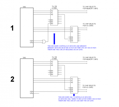
If you're using a circuit more or less like that in the upper part of this image then yes, the OR gate is required. I've shown 138's, but the same idea applies using other decoders, or programmable logic. The salient aspect is that the qualifying signal gets injected at a point where both I/O and memory are affected. Memory devices may contain code, and therefore they must be allowed to be active anytime VPA or VDA is high. The OR gate ensures that this is the case.
Attachment:
 VDA injection points.png [ 15.6 KiB | Viewed 412 times ]
However, no OR gate is required for the circuit in the lower part of the image because the qualifying signal gets injected further downstream at a point where only I/O is affected. I/O devices don't contain code, and it's sufficient that they merely be allowed to be active when VDA is high. This means VPA can be ignored and the OR gate omitted, resulting in simpler, faster logic. The difference may not be enough to sway
you, and it's alright if you don't do it this way. But every decision is a tradeoff, and for other folks the various factors may evaluate to a different outcome. Both circuits protect the I/O devices from spurious access during dead cycles.
I hope it's clear that I'm not saying that the upper circuit is wrong, or that wait-stated ROM is wrong; only saying that the tradeoffs will vary from one situation to the next. For example, I don't deny that using VPA on your POC only tied up one pin on the CPLD. But someone in a different situation may need that pin for something else, or perhaps may not be using programmable logic at all. Your circumstances and priorities don't necessarily match those of other builders.
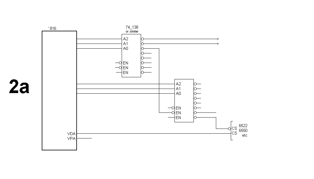
Finally, here's a circuit variation that injects the qualifying signal even further downstream -- ie, at the I/O device itself! This is a zero-cost alternative for cases when you're using 65xx I/O chips and you're not otherwise using the active-high chip selects.
Attachment:
 VDA injection point for 65xx I-O.png [ 6.5 KiB | Viewed 410 times ]
-- Jeff
[Edits]


