6502.org Forum  Projects  Code  Documents  Tools  Forum
It is currently Wed May 08, 2024 6:24 pm

All times are UTC


Post new topic Reply to topic  [ 298 posts ]  Go to page Previous  1 ... 16, 17, 18, 19, 20
Author Message
PostPosted: Tue May 19, 2020 7:13 pm 
Offline
User avatar

Joined: Fri Aug 03, 2018 8:52 am
Posts: 746
Location: Germany
Ok so finally i got the parts from Mouser and was able to get soldering.
Yesterday i only had enough time to solder my breakout board for the ATF1504. but that was already since it gave me the rest of the day to experiment with JTAG...
and man, JTAG Programming is so easy, why did i never use CPLDs before?!
Today i was able to solder the SBC, and i was atleast able to verify that a PC recognized the FT240X when plugging it in. which is already better than last time.

here some pictures of the finished boards:
Attachment:
20200519_201117.jpg
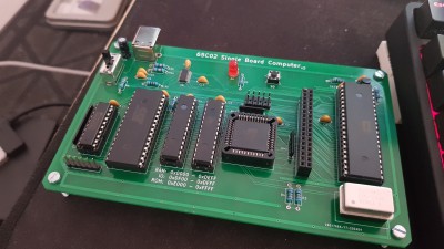
20200519_201117.jpg [ 2.96 MiB | Viewed 1309 times ]

Attachment:
20200519_201132.jpg
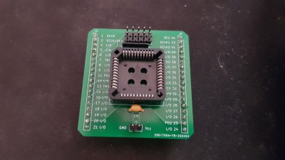
20200519_201132.jpg [ 2.68 MiB | Viewed 1309 times ]

also, side note, what's with this site liking to log me out when i upload a file?
i refresh the site before i post a reply to make sure i'm still logged in but as soon as i upload a file i get logged out...
maybe i just forget how long i take to get pictures off my phone before actually uploading them? but that would be weird timing since it happend atleast 3 times already.

anyways i was excited to test the SBC out, so i got my small Hello World Program, put it on the flash chip and let it run...

aaaaand like expected, nothing happend.
after a bit of debugging i found 2 problems, and both are so stupid i want to punch myself.

just take a look at the current schematic:
Attachment:
chrome_2020-05-19_21-02-42.png
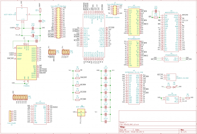
chrome_2020-05-19_21-02-42.png [ 519.23 KiB | Viewed 1309 times ]

there are (currently) 2 obvious mistakes i somehow didn't notice before ordering the PCBs...
1. at the bottom middle, notice the Oscillator... and that very distant Vcc to the right of it? yep, i forgot to move it back before routing, leaving the Oscillator without power
2. at the top right, that little circuit for the RDY pin, it connects to that "/RDY" network.... and that's it. there is no counterpart, it doesn't connect to anything. not even the large connector in the top left... leaving the RDY pin floating...

this means 2 botch wires will have to be soldered tomorrow. dammit, i hoped i would get through this one without mistakes!
though i'm not 100% sure where to solder the RDY pin to, i could just connect it to Vcc, or the CPLD, in case there somehow is a RDY circuit that can fit into there that i could use.
but i'll probably just solder it to Vcc.

man i want to do an FPGA based VGA card for this thing after this but i cannot even get the base PCB correct... (btw that will be it's own thread)

oh well, tomorrow i will report back with a hopefully working SBC...


Top
 Profile  
Reply with quote  
PostPosted: Wed May 20, 2020 8:08 am 
Offline

Joined: Tue Sep 03, 2002 12:58 pm
Posts: 298
/RDY is bidirectional on the 65C02, so it would be best to pull it high through a resistor. Anything that needs to pull it low can do so through an open-drain output.


Top
 Profile  
Reply with quote  
PostPosted: Wed May 20, 2020 11:47 am 
Offline
User avatar

Joined: Fri Aug 03, 2018 8:52 am
Posts: 746
Location: Germany
John West wrote:
/RDY is bidirectional on the 65C02, so it would be best to pull it high through a resistor. Anything that needs to pull it low can do so through an open-drain output.


yes that is why it has a resistor and capacitor on the schematic.

.

so i soldered the 2 wires but i'm still having problems.

using my arduino logic probe i can see it's trying to do things but the data it's reading doesn't make much sense. i think something must be wrong in my CPLD.

it seems to be decoding RAM/ROM correctly but the IO divices also output their data at times despite the address not being correct...

here is the code of the CPLD, i also checked all of the pins and they correspond with what is on the Schematic/PCB.

Code:
Name        65C02_SBC_v2;
PartNo      00;
Date        31.03.2020;
Revision    01;
Designer    None;
Company     None;
Assembly    None;
Location    None;
Device      f1504ispplcc44;

property   atmel {pin_keep=off};
property   atmel {security=off};

/* *************** INPUT PINS **********************/

PIN      1   = SYS_RST;
PIN      43   = SYS_CLK;
PIN      21   = RW;            /* Read(1) Write(0) */
PIN      27   = A0;
PIN      28   = A1;
PIN      29   = A2;
PIN      31   = A3;
PIN      33   = A4;
PIN      34   = A5;
PIN      36   = A6;
PIN      37   = A7;
PIN      20   = A8;
PIN      19   = A9;
PIN      18   = A10;
PIN      17   = A11;
PIN      16   = A12;
PIN      24   = A13;
PIN      25   = A14;
PIN      26   = A15;
PIN      40   = DIS_ROM;
PIN      39   = DIS_RAM;

/* *************** OUTPUT PINS *********************/

PIN         = !RDY;
PIN      12   = !OE_MEM;
PIN      14   = !WE_MEM;
PIN      11   = !CS_ROM;
PIN      9   = !CS_RAM_0;
PIN      8   = !CS_RAM_1;
PIN      4   = !RD_FT240X;
PIN      6   = WR_FT240X;
PIN      5   = !RD_STATUS;


/* ****************** LOGIC ************************/

/* Memory R/W */

OE_MEM   = (SYS_CLK & RW);
WE_MEM   = (SYS_CLK & !RW);

/* Memory Map */

CS_ROM   = A15 & A14 & A13 & DIS_ROM;
IO_EN    = A15 & A14 & !A13 & A12 & A11 & A10 & A9 & A8;
CS_RAM_0 = !CS_ROM & !IO_EN & !A15 & DIS_RAM;
CS_RAM_1 = !CS_ROM & !IO_EN & A15 & DIS_RAM;

/* IO Devices */

RD_STATUS = !IO_EN & !(A7 & A6 & A5 & A4 & A3 & A2 & A1) & A0 & SYS_CLK & RW;
RD_FT240X = !IO_EN & !(A7 & A6 & A5 & A4 & A3 & A2 & A1) & !A0 & SYS_CLK & RW;
WR_FT240X = !IO_EN & !(A7 & A6 & A5 & A4 & A3 & A2 & A1) & !A0 & SYS_CLK & !RW;


overall the memory map should look like this:

0x0000 - 0xDEFF -> RAM
0xDF00 - 0xDFFF -> IO (0xDF00 for the "FT240X" and 0xDF01 for the "STATUS")
0xE000 - 0xFFFF -> ROM

RAM is technically covering the whole 64k, so any writes done to anywhere in the address range will always write to RAM, even if it's also writting to an IO Device or ROM.
reading on the other hand is always done from whatever is currently accessed, either RAM, IO, or ROM. never multiple at the same time.

what's up here? it suddendly feels so empty...


Top
 Profile  
Reply with quote  
PostPosted: Wed May 20, 2020 1:28 pm 
Offline

Joined: Mon May 21, 2018 8:09 pm
Posts: 1462
Normally you produce global /OE and /WE signals that are connected to every device, and use /CE to select just the single device that you want to respond to each address. That is not what you have set up here…


Top
 Profile  
Reply with quote  
PostPosted: Wed May 20, 2020 1:48 pm 
Offline
User avatar

Joined: Fri Aug 03, 2018 8:52 am
Posts: 746
Location: Germany
Chromatix wrote:
Normally you produce global /OE and /WE signals that are connected to every device, and use /CE to select just the single device that you want to respond to each address. That is not what you have set up here…


is it not? because that is exactly what i wanted to do.

OE and WE are just tied to the clock and the RW pin of the CPU, the CS is purely dependent on the Address. (and technically the DIS_RAM and DIS_ROM inputs, which are always 1 in this case)

only exception are the IO Devices, which only have OE/WE pins, so their pins depend on the Address, Clock, and RW.

it is exactly how it worked before when i had 2 seperate GALs.


Top
 Profile  
Reply with quote  
PostPosted: Wed May 20, 2020 4:07 pm 
Offline

Joined: Mon May 21, 2018 8:09 pm
Posts: 1462
Right, most I/O devices have /CE, /OE and /WE signals (perhaps under different names and occasionally with different polarity), specifically because that matches the usual convention for attaching to a CPU bus. That the FTDI device does not is very unusual.

It would be reasonable to insert a couple of external 2-OR gates to generate "local" /RD and /WR signals for a specific device of that type, using the global /OE and /WE and the device-specific /CE. In CUPL you can simulate this (to simplify the code) with internal "virtual" signal nodes, which are then used as part of another equation, and the compiler will sort out the details to make it fit in the device.


Top
 Profile  
Reply with quote  
PostPosted: Wed May 20, 2020 6:20 pm 
Offline
User avatar

Joined: Fri Aug 03, 2018 8:52 am
Posts: 746
Location: Germany
Chromatix wrote:
Right, most I/O devices have /CE, /OE and /WE signals (perhaps under different names and occasionally with different polarity), specifically because that matches the usual convention for attaching to a CPU bus. That the FTDI device does not is very unusual.

It would be reasonable to insert a couple of external 2-OR gates to generate "local" /RD and /WR signals for a specific device of that type, using the global /OE and /WE and the device-specific /CE. In CUPL you can simulate this (to simplify the code) with internal "virtual" signal nodes, which are then used as part of another equation, and the compiler will sort out the details to make it fit in the device.


but, i got a CPLD, shouldn't it be more reasonable to just use that instead of adding actual gates?
I mean what you're desrcibing is pretty much what the code above is already doing, or atleast trying to do.

and this way i'm currently using it is pretty much identical to how i did it with the 2 GALs on the previous board, just as one chip, and it worked perfectly fine on the other board...

one GAL would decode the upper half of the address bus to generate the CS signals for RAM, ROM, and IO. And the OE and WE signals for Memory.
the IO CS would go into the second GAL to decode the lower half of the address bus to generate the OE and WE signals for the FT240X and the STATUS.

but for some reason it doesn't seem to work.

I think i'll just pop out the CPLD, put it into my breakout board, hook it up to my arduino and just run a few tests with it.
i tried to use WinCUPL's simulation thingy, but it just said there were errors, but the error counter is 0 with a bunch of warnings...
and i'd rather just program my own tests i can do with the hardware then to try to get some outdated software to work...


Top
 Profile  
Reply with quote  
PostPosted: Wed May 20, 2020 6:24 pm 
Offline
User avatar

Joined: Thu Dec 11, 2008 1:28 pm
Posts: 10800
Location: England
What kind of instruments or diagnostic tools do you have, @proxy?

Ideally you'd have a scope or logic analyser and see both the logic activity and the relative timing.


Top
 Profile  
Reply with quote  
PostPosted: Wed May 20, 2020 6:42 pm 
Offline
User avatar

Joined: Fri Aug 03, 2018 8:52 am
Posts: 746
Location: Germany
BigEd wrote:
What kind of instruments or diagnostic tools do you have, @proxy?

Ideally you'd have a scope or logic analyser and see both the logic activity and the relative timing.


the only thing i have is an Arduino Mega i use as a poor man's logic analyzer. it generates the clock itself so that everything is synchronized and outputs the data in the following format:

A: 0x0000 D: 0x00 RD/WR HIGH/LOW

first the address, then the current data on the bus, the if the CPU is Reading or Writing, and lastly it shows the current clock state.

The obvious downside is that i cannot use it to find timing issues as i cannot run the system regular operation speeds (>1MHz) without the arduino falling behind.
But it's enough to test all the hardware without having to worry about timing constraits. (and the system seems to be already failing at just working in general even at ~1Hz)

and next up i wanted to use another Arduino to test the CPLD itself, basically just giving it a specific address, RW signal, and CLK signal, and then comparing the outputted CS/OE/WE/etc signals with what i expect them to be.


Top
 Profile  
Reply with quote  
PostPosted: Wed May 20, 2020 7:06 pm 
Offline
User avatar

Joined: Thu Dec 11, 2008 1:28 pm
Posts: 10800
Location: England
Quote:
using my arduino logic probe i can see it's trying to do things but the data it's reading doesn't make much sense. i think something must be wrong in my CPLD.

it seems to be decoding RAM/ROM correctly but the IO divices also output their data at times despite the address not being correct...

So the program flow is as expected, but you suspect the address decoding? Checking the CPLD truth table sounds like a good idea. Drawing out what you expect to see for typical accesses might help too.

It could easily be a matter of timing: that your logic isn't qualifying signals appropriately and adjacent accesses are overlapping. Or your Arduino is sampling or acting at the wrong point in the clock cycle.


Top
 Profile  
Reply with quote  
PostPosted: Wed May 20, 2020 7:22 pm 
Offline
User avatar

Joined: Fri Aug 03, 2018 8:52 am
Posts: 746
Location: Germany
BigEd wrote:
Quote:
using my arduino logic probe i can see it's trying to do things but the data it's reading doesn't make much sense. i think something must be wrong in my CPLD.

it seems to be decoding RAM/ROM correctly but the IO divices also output their data at times despite the address not being correct...

So the program flow is as expected, but you suspect the address decoding? Checking the CPLD truth table sounds like a good idea. Drawing out what you expect to see for typical accesses might help too.

It could easily be a matter of timing: that your logic isn't qualifying signals appropriately and adjacent accesses are overlapping. Or your Arduino is sampling or acting at the wrong point in the clock cycle.


the program flow is not correct either, while the CS signals for RAM and ROM seem correct the actual data that gets put on the bus doesn't correspond to what the ROM should have at that address.

i assume it's because of the IO Devices "randomly" throwing their data onto the bus that screws it up.

the arduino program works as follows:
1. read in the current status of the Address bus, Data bus, RW pin, and Clock state
2. switch the clock state (and output the state of the clock to the LED on the Arduino board)
3. wait a specific amount of time (uses an analog input to calculate the waiting so i can control it via a Potentiometer)
4. goto 1

since the waiting happens after the clock changes it should ensure that everything has more than enough time to give a stable output before everything is sampled again.

and looking at the look up table just confuses me but at the same time it seems to confirm my suspicion.
the "RD_FT240X", "WR_FT240X", and "RD_STATUS" outputs should only have a single possible way that they could be active, since they correspond to exactly one address and one state of the clock and RW input.

buuut:

Code:
*******************************************************************************
                                 65C02_SBC_v2
*******************************************************************************

CUPL(WM)        5.0a Serial# 60008009
Device          f1504ispplcc44  Library DLIB-h-40-1
Created         Wed May 20 21:21:20 2020
Name            65C02_SBC_v2
Partno          00
Revision        01
Date            31.03.2020
Designer        None
Company         None
Assembly        None
Location        None

===============================================================================
                            Expanded Product Terms
===============================================================================

CS_RAM_0 =>
    !A15 & !CS_ROM & DIS_RAM

CS_RAM_1 =>
    !A8 & A15 & !CS_ROM & DIS_RAM
  # !A9 & A15 & !CS_ROM & DIS_RAM
  # !A10 & A15 & !CS_ROM & DIS_RAM
  # !A11 & A15 & !CS_ROM & DIS_RAM
  # !A12 & A15 & !CS_ROM & DIS_RAM
  # A13 & A15 & !CS_ROM & DIS_RAM
  # !A14 & A15 & !CS_ROM & DIS_RAM

CS_ROM =>
    A13 & A14 & A15 & DIS_ROM

IO_EN =>
    A8 & A9 & A10 & A11 & A12 & !A13 & A14 & A15

OE_MEM =>
    RW & SYS_CLK

RD_FT240X =>
    !A0 & !A1 & !A8 & RW & SYS_CLK
  # !A0 & !A2 & !A8 & RW & SYS_CLK
  # !A0 & !A3 & !A8 & RW & SYS_CLK
  # !A0 & !A4 & !A8 & RW & SYS_CLK
  # !A0 & !A5 & !A8 & RW & SYS_CLK
  # !A0 & !A6 & !A8 & RW & SYS_CLK
  # !A0 & !A7 & !A8 & RW & SYS_CLK
  # !A0 & !A1 & !A9 & RW & SYS_CLK
  # !A0 & !A2 & !A9 & RW & SYS_CLK
  # !A0 & !A3 & !A9 & RW & SYS_CLK
  # !A0 & !A4 & !A9 & RW & SYS_CLK
  # !A0 & !A5 & !A9 & RW & SYS_CLK
  # !A0 & !A6 & !A9 & RW & SYS_CLK
  # !A0 & !A7 & !A9 & RW & SYS_CLK
  # !A0 & !A1 & !A10 & RW & SYS_CLK
  # !A0 & !A2 & !A10 & RW & SYS_CLK
  # !A0 & !A3 & !A10 & RW & SYS_CLK
  # !A0 & !A4 & !A10 & RW & SYS_CLK
  # !A0 & !A5 & !A10 & RW & SYS_CLK
  # !A0 & !A6 & !A10 & RW & SYS_CLK
  # !A0 & !A7 & !A10 & RW & SYS_CLK
  # !A0 & !A1 & !A11 & RW & SYS_CLK
  # !A0 & !A2 & !A11 & RW & SYS_CLK
  # !A0 & !A3 & !A11 & RW & SYS_CLK
  # !A0 & !A4 & !A11 & RW & SYS_CLK
  # !A0 & !A5 & !A11 & RW & SYS_CLK
  # !A0 & !A6 & !A11 & RW & SYS_CLK
  # !A0 & !A7 & !A11 & RW & SYS_CLK
  # !A0 & !A1 & !A12 & RW & SYS_CLK
  # !A0 & !A2 & !A12 & RW & SYS_CLK
  # !A0 & !A3 & !A12 & RW & SYS_CLK
  # !A0 & !A4 & !A12 & RW & SYS_CLK
  # !A0 & !A5 & !A12 & RW & SYS_CLK
  # !A0 & !A6 & !A12 & RW & SYS_CLK
  # !A0 & !A7 & !A12 & RW & SYS_CLK
  # !A0 & !A1 & A13 & RW & SYS_CLK
  # !A0 & !A2 & A13 & RW & SYS_CLK
  # !A0 & !A3 & A13 & RW & SYS_CLK
  # !A0 & !A4 & A13 & RW & SYS_CLK
  # !A0 & !A5 & A13 & RW & SYS_CLK
  # !A0 & !A6 & A13 & RW & SYS_CLK
  # !A0 & !A7 & A13 & RW & SYS_CLK
  # !A0 & !A1 & !A14 & RW & SYS_CLK
  # !A0 & !A2 & !A14 & RW & SYS_CLK
  # !A0 & !A3 & !A14 & RW & SYS_CLK
  # !A0 & !A4 & !A14 & RW & SYS_CLK
  # !A0 & !A5 & !A14 & RW & SYS_CLK
  # !A0 & !A6 & !A14 & RW & SYS_CLK
  # !A0 & !A7 & !A14 & RW & SYS_CLK
  # !A0 & !A1 & !A15 & RW & SYS_CLK
  # !A0 & !A2 & !A15 & RW & SYS_CLK
  # !A0 & !A3 & !A15 & RW & SYS_CLK
  # !A0 & !A4 & !A15 & RW & SYS_CLK
  # !A0 & !A5 & !A15 & RW & SYS_CLK
  # !A0 & !A6 & !A15 & RW & SYS_CLK
  # !A0 & !A7 & !A15 & RW & SYS_CLK

RD_STATUS =>
    A0 & !A1 & !A8 & RW & SYS_CLK
  # A0 & !A2 & !A8 & RW & SYS_CLK
  # A0 & !A3 & !A8 & RW & SYS_CLK
  # A0 & !A4 & !A8 & RW & SYS_CLK
  # A0 & !A5 & !A8 & RW & SYS_CLK
  # A0 & !A6 & !A8 & RW & SYS_CLK
  # A0 & !A7 & !A8 & RW & SYS_CLK
  # A0 & !A1 & !A9 & RW & SYS_CLK
  # A0 & !A2 & !A9 & RW & SYS_CLK
  # A0 & !A3 & !A9 & RW & SYS_CLK
  # A0 & !A4 & !A9 & RW & SYS_CLK
  # A0 & !A5 & !A9 & RW & SYS_CLK
  # A0 & !A6 & !A9 & RW & SYS_CLK
  # A0 & !A7 & !A9 & RW & SYS_CLK
  # A0 & !A1 & !A10 & RW & SYS_CLK
  # A0 & !A2 & !A10 & RW & SYS_CLK
  # A0 & !A3 & !A10 & RW & SYS_CLK
  # A0 & !A4 & !A10 & RW & SYS_CLK
  # A0 & !A5 & !A10 & RW & SYS_CLK
  # A0 & !A6 & !A10 & RW & SYS_CLK
  # A0 & !A7 & !A10 & RW & SYS_CLK
  # A0 & !A1 & !A11 & RW & SYS_CLK
  # A0 & !A2 & !A11 & RW & SYS_CLK
  # A0 & !A3 & !A11 & RW & SYS_CLK
  # A0 & !A4 & !A11 & RW & SYS_CLK
  # A0 & !A5 & !A11 & RW & SYS_CLK
  # A0 & !A6 & !A11 & RW & SYS_CLK
  # A0 & !A7 & !A11 & RW & SYS_CLK
  # A0 & !A1 & !A12 & RW & SYS_CLK
  # A0 & !A2 & !A12 & RW & SYS_CLK
  # A0 & !A3 & !A12 & RW & SYS_CLK
  # A0 & !A4 & !A12 & RW & SYS_CLK
  # A0 & !A5 & !A12 & RW & SYS_CLK
  # A0 & !A6 & !A12 & RW & SYS_CLK
  # A0 & !A7 & !A12 & RW & SYS_CLK
  # A0 & !A1 & A13 & RW & SYS_CLK
  # A0 & !A2 & A13 & RW & SYS_CLK
  # A0 & !A3 & A13 & RW & SYS_CLK
  # A0 & !A4 & A13 & RW & SYS_CLK
  # A0 & !A5 & A13 & RW & SYS_CLK
  # A0 & !A6 & A13 & RW & SYS_CLK
  # A0 & !A7 & A13 & RW & SYS_CLK
  # A0 & !A1 & !A14 & RW & SYS_CLK
  # A0 & !A2 & !A14 & RW & SYS_CLK
  # A0 & !A3 & !A14 & RW & SYS_CLK
  # A0 & !A4 & !A14 & RW & SYS_CLK
  # A0 & !A5 & !A14 & RW & SYS_CLK
  # A0 & !A6 & !A14 & RW & SYS_CLK
  # A0 & !A7 & !A14 & RW & SYS_CLK
  # A0 & !A1 & !A15 & RW & SYS_CLK
  # A0 & !A2 & !A15 & RW & SYS_CLK
  # A0 & !A3 & !A15 & RW & SYS_CLK
  # A0 & !A4 & !A15 & RW & SYS_CLK
  # A0 & !A5 & !A15 & RW & SYS_CLK
  # A0 & !A6 & !A15 & RW & SYS_CLK
  # A0 & !A7 & !A15 & RW & SYS_CLK

WE_MEM =>
    !RW & SYS_CLK

WR_FT240X =>
    !A0 & !A1 & !A8 & !RW & SYS_CLK
  # !A0 & !A2 & !A8 & !RW & SYS_CLK
  # !A0 & !A3 & !A8 & !RW & SYS_CLK
  # !A0 & !A4 & !A8 & !RW & SYS_CLK
  # !A0 & !A5 & !A8 & !RW & SYS_CLK
  # !A0 & !A6 & !A8 & !RW & SYS_CLK
  # !A0 & !A7 & !A8 & !RW & SYS_CLK
  # !A0 & !A1 & !A9 & !RW & SYS_CLK
  # !A0 & !A2 & !A9 & !RW & SYS_CLK
  # !A0 & !A3 & !A9 & !RW & SYS_CLK
  # !A0 & !A4 & !A9 & !RW & SYS_CLK
  # !A0 & !A5 & !A9 & !RW & SYS_CLK
  # !A0 & !A6 & !A9 & !RW & SYS_CLK
  # !A0 & !A7 & !A9 & !RW & SYS_CLK
  # !A0 & !A1 & !A10 & !RW & SYS_CLK
  # !A0 & !A2 & !A10 & !RW & SYS_CLK
  # !A0 & !A3 & !A10 & !RW & SYS_CLK
  # !A0 & !A4 & !A10 & !RW & SYS_CLK
  # !A0 & !A5 & !A10 & !RW & SYS_CLK
  # !A0 & !A6 & !A10 & !RW & SYS_CLK
  # !A0 & !A7 & !A10 & !RW & SYS_CLK
  # !A0 & !A1 & !A11 & !RW & SYS_CLK
  # !A0 & !A2 & !A11 & !RW & SYS_CLK
  # !A0 & !A3 & !A11 & !RW & SYS_CLK
  # !A0 & !A4 & !A11 & !RW & SYS_CLK
  # !A0 & !A5 & !A11 & !RW & SYS_CLK
  # !A0 & !A6 & !A11 & !RW & SYS_CLK
  # !A0 & !A7 & !A11 & !RW & SYS_CLK
  # !A0 & !A1 & !A12 & !RW & SYS_CLK
  # !A0 & !A2 & !A12 & !RW & SYS_CLK
  # !A0 & !A3 & !A12 & !RW & SYS_CLK
  # !A0 & !A4 & !A12 & !RW & SYS_CLK
  # !A0 & !A5 & !A12 & !RW & SYS_CLK
  # !A0 & !A6 & !A12 & !RW & SYS_CLK
  # !A0 & !A7 & !A12 & !RW & SYS_CLK
  # !A0 & !A1 & A13 & !RW & SYS_CLK
  # !A0 & !A2 & A13 & !RW & SYS_CLK
  # !A0 & !A3 & A13 & !RW & SYS_CLK
  # !A0 & !A4 & A13 & !RW & SYS_CLK
  # !A0 & !A5 & A13 & !RW & SYS_CLK
  # !A0 & !A6 & A13 & !RW & SYS_CLK
  # !A0 & !A7 & A13 & !RW & SYS_CLK
  # !A0 & !A1 & !A14 & !RW & SYS_CLK
  # !A0 & !A2 & !A14 & !RW & SYS_CLK
  # !A0 & !A3 & !A14 & !RW & SYS_CLK
  # !A0 & !A4 & !A14 & !RW & SYS_CLK
  # !A0 & !A5 & !A14 & !RW & SYS_CLK
  # !A0 & !A6 & !A14 & !RW & SYS_CLK
  # !A0 & !A7 & !A14 & !RW & SYS_CLK
  # !A0 & !A1 & !A15 & !RW & SYS_CLK
  # !A0 & !A2 & !A15 & !RW & SYS_CLK
  # !A0 & !A3 & !A15 & !RW & SYS_CLK
  # !A0 & !A4 & !A15 & !RW & SYS_CLK
  # !A0 & !A5 & !A15 & !RW & SYS_CLK
  # !A0 & !A6 & !A15 & !RW & SYS_CLK
  # !A0 & !A7 & !A15 & !RW & SYS_CLK


this program hates me.


Top
 Profile  
Reply with quote  
PostPosted: Wed May 20, 2020 7:33 pm 
Offline
User avatar

Joined: Wed Feb 14, 2018 2:33 pm
Posts: 1405
Location: Scotland
Proxy wrote:
but for some reason it doesn't seem to work.


I'm going to assume you've done this already, but if not ...

Using your multimeter that has a beep/continuity tester, then you'd do what we used to call "buzzing out" a board. Remove all the chips then go through each chip socket one at a time. One probe in pin 1, then run the other probe down both sides to make sure there are no unintentional shorts. Do this for each DIL socket. Check power continuity from the power input to each component.

Another thing you can do is connect a flying lead to a spare input pin on the ATmega and an LED to a spare output pin and as part of your polling loop, add that pin into it and reflect its status on the LED - and you have a free logic probe. (Make sure the input pin is configured with the internal pull-up turned off) Use that to double-check the state of BE, Rdy, IRQ and so on.

Remove all peripherals - leave just the 65C02.

Program the 8 pins you are using for the data bus monitor on the ATmega as outputs and jam EA on it. You now have a NOP generator. Clock the 6502 and watch the address bus count up binary fashion.

That might give some insight. Good luck!

Gordon

_________________
--
Gordon Henderson.
See my Ruby 6502 and 65816 SBC projects here: https://projects.drogon.net/ruby/


Top
 Profile  
Reply with quote  
PostPosted: Wed May 20, 2020 8:20 pm 
Offline
User avatar

Joined: Fri Aug 03, 2018 8:52 am
Posts: 746
Location: Germany
drogon wrote:
Proxy wrote:
but for some reason it doesn't seem to work.


I'm going to assume you've done this already, but if not ...

Using your multimeter that has a beep/continuity tester, then you'd do what we used to call "buzzing out" a board. Remove all the chips then go through each chip socket one at a time. One probe in pin 1, then run the other probe down both sides to make sure there are no unintentional shorts. Do this for each DIL socket. Check power continuity from the power input to each component.

Another thing you can do is connect a flying lead to a spare input pin on the ATmega and an LED to a spare output pin and as part of your polling loop, add that pin into it and reflect its status on the LED - and you have a free logic probe. (Make sure the input pin is configured with the internal pull-up turned off) Use that to double-check the state of BE, Rdy, IRQ and so on.

Remove all peripherals - leave just the 65C02.

Program the 8 pins you are using for the data bus monitor on the ATmega as outputs and jam EA on it. You now have a NOP generator. Clock the 6502 and watch the address bus count up binary fashion.

That might give some insight. Good luck!

Gordon


luckly that doesn't seem nessesary... as said the IO EO/WE signals should have exactly one way to activate, but as the file showed they clearly have more
after fixing the code (which actually took a bit of rethinking) it seems fine now:

Code:
*******************************************************************************
                                 65C02_SBC_v2
*******************************************************************************

CUPL(WM)        5.0a Serial# 60008009
Device          f1504ispplcc44  Library DLIB-h-40-1
Created         Wed May 20 21:53:11 2020
Name            65C02_SBC_v2
Partno          00
Revision        01
Date            31.03.2020
Designer        None
Company         None
Assembly        None
Location        None

===============================================================================
                            Expanded Product Terms
===============================================================================

CS_RAM_0 =>
    !A15 & !CS_ROM & DIS_RAM

CS_RAM_1 =>
    !A8 & A15 & !CS_ROM & DIS_RAM
  # !A9 & A15 & !CS_ROM & DIS_RAM
  # !A10 & A15 & !CS_ROM & DIS_RAM
  # !A11 & A15 & !CS_ROM & DIS_RAM
  # !A12 & A15 & !CS_ROM & DIS_RAM
  # A13 & A15 & !CS_ROM & DIS_RAM
  # !A14 & A15 & !CS_ROM & DIS_RAM

CS_ROM =>
    A13 & A14 & A15 & DIS_ROM

IO_EN =>
    A8 & A9 & A10 & A11 & A12 & !A13 & A14 & A15

OE_MEM =>
    RW & SYS_CLK

RD_FT240X =>
    !A0 & !A1 & !A2 & !A3 & !A4 & !A5 & !A6 & !A7 & A8 & A9 & A10 & A11 & A12 &
      !A13 & A14 & A15 & RW & SYS_CLK

RD_STATUS =>
    A0 & !A1 & !A2 & !A3 & !A4 & !A5 & !A6 & !A7 & A8 & A9 & A10 & A11 & A12 &
      !A13 & A14 & A15 & RW & SYS_CLK

WE_MEM =>
    !RW & SYS_CLK

WR_FT240X =>
    !A0 & !A1 & !A2 & !A3 & !A4 & !A5 & !A6 & !A7 & A8 & A9 & A10 & A11 & A12 &
      !A13 & A14 & A15 & !RW & SYS_CLK


and more importantly, the SBC seems to work as well!
i got a small echo program running that just waits for data from the FT240X, once it has something the CPU reads it out and sends it back to the FT240X
it has a noticable delay when clicking keys in irregular patterns, but that is kinda expected from the wait loops i use to check for data being there...

if anyone remembers i used to have a problem where the Status byte would sometimes spit out incorrect data, making it seem like data was in the FT240X even though there was nothing.
well that seems to be gone now as well, i had the SBC sit actively checking for data while writing this and it didn't spit out any random null bytes so that's good.

now i can actually start programming something without worrying that the hardware might be faulty, yay!

though i still have to do one last botch wire, i somehow got a 3rd mistake in my design, but luckly this one doesn't effect the function of the actual computer, i just had the wrong network name for the RW pin on the Pin header in the middle of the board. so that was not connected to anything... which explains why my logic analyzer was only showing the CPU reading data... because it wasn't actually connected to the CPU...
and i can't have a broken RW pin on the pin header, i wanna use that for expansion cards in the future!

very much thank you everyone helping me out with this, i should've checked the LOG file much earlier but i just didn't think of it...


Top
 Profile  
Reply with quote  
Display posts from previous:  Sort by  
Post new topic Reply to topic  [ 298 posts ]  Go to page Previous  1 ... 16, 17, 18, 19, 20

All times are UTC


Who is online

Users browsing this forum: No registered users and 4 guests


You cannot post new topics in this forum
You cannot reply to topics in this forum
You cannot edit your posts in this forum
You cannot delete your posts in this forum
You cannot post attachments in this forum

Search for:
Jump to: