6502.org Forum  Projects  Code  Documents  Tools  Forum
It is currently Wed Apr 24, 2024 11:26 am

All times are UTC


Post new topic Reply to topic  [ 47 posts ]  Go to page 1, 2, 3, 4  Next
Author Message
PostPosted: Tue Apr 10, 2018 8:00 am 
Offline
User avatar

Joined: Mon Apr 09, 2018 11:33 am
Posts: 19
Location: Free Country, USA
Greetings! I'm surprised I didn't visit this forum sooner. I'm not really sure where to start with all of this so here goes the short story of The Cactus.

Attachment:
File comment: Front panels are pretty
IMG_20180227_043657595.jpg
IMG_20180227_043657595.jpg [ 3.2 MiB | Viewed 7020 times ]


A few years ago, I saw an OSI-300 on display at VCF East. I had never seen a 6502 machine that was so spartan, and more importantly was using toggle switches and LEDs instead of a hex keypad/display, with a ROM to help you out. Other processors commonly had front panel interfaces, but why not 6502's?

I wanted an OSI-300, but I knew they were prohibitively rare. I briefly thought I could make my own, but the lack of a schematic and the awareness of my own ignorance made the task a bit too daunting. The good news was that within 6 months, a mini OSI-300 kit was available so I bought a pair. It was eye opening and fun, but the tiny switches made it tough for me to use for more than a few minutes. I figured I could make a few changes to it and improve the usability.

Some time later, I saw Grant Searle's low-chip count 6502 design with serial and BASIC aboard and wondered if the two concepts could be united, Altair 680 style.

That idea spiraled out of control. I started designing schematics for a complicated front panel interface that had features I figured would be nice. Things like:
  • Hopping to an address location, then incrementing with the press of a button.
  • Viewing, modifying, and re-entering bytes on the data bus, without having to re-enter the entire byte. Say you mistakenly entered 2C instead of 2D? Rather than clear the entire byte Kenbak-1 style, just change the bit that you messed up.
  • Set/Clear momentary switches, like an HP-1000 which I got to experience at VCF MW last year.
  • Observing the data and address buses while the CPU is running for maximum blinkenlights.
  • Features like Deposit, Deposit Next, Examine, and Examine Next.
  • Modular cards, to allow easy improvements.
  • Slow clock speed, right around 1MHz to allow use of older components.
  • Single stepping the CPU (the one thing I know is considered to be the most unlikely goal on a 6502)

So for the last year, I've been hard at work designing and building my machine, piece by piece. My starting point was to separate Grant's design into individual cards and put them on a backplane. I breadboarded his design as a test article, then modified it slightly to match the baud rates I would be using. I upgraded to a modern WD65C02S for kicks (from an old NMOS Commodore made 6502), only to discover that the modern ones have a Bus Enable pin, and a static core which might make my single stepping dream come true.

Attachment:
File comment: The 7 cards I've built so far. Top row: 32K RAM, 16K EPROM, selectable baud rate serial card, address control card.
Bottom row: CPU card, status control card, data control card.

IMG_20180327_014229932.jpg
IMG_20180327_014229932.jpg [ 3.25 MiB | Viewed 7020 times ]


I constructed front panel interface cards, one at a time, resulting in 7 cards. 32K RAM, 16K EPROM, selectable baud rate serial card, address control card, CPU card, status control card, data control card. While the CPU is running, the front panel logic cards are supposed to sit quiet and observe the bus but not interfere. When the CPU is halted, they are to unlock and let you visit addresses, observe and modify data, and otherwise play... that's the idea anyway.

Attachment:
File comment: Early integration tests sans CPU.
IMG_20180313_244927707.jpg
IMG_20180313_244927707.jpg [ 2.69 MiB | Viewed 7020 times ]


In practice it doesn't go that well. While testing the data control and address control cards individually, they seem to work fine. In integration testing, they fail to do their jobs, and produce phantom operations. The status control card is another story, that thing is riddled with problems, but it can be bypassed for the moment. Other tests have involved just the CPU, RAM, ROM, and serial, with all of the extra features disabled. For these tests, things like the single step is hard wired out, along with the more precise address decoding of the serial card. Effectively, it's supposed to be just the breadboarded Grant Searle design but on my backplane & cards. No dice. Every time, it looks like it gets just past checking the reset vector and then produces inconstant results on each test run.

I know there are aspects to the implementation and design process where my knowledge is lacking. I'm walking into a world where I have never tread before, and thus there is much to learn. I've discovered much but hit a bit of a road block. Right now, my current plan of attack is to observe most of the bus with a simple logic analyzer, and see where the hiccups are. I've also got a hunch that the bus signals are ringing, and thus possibly poorly terminated, but I don't have enough evidence to back that up or what I would do about it. I'm not really sure where to go from here. I'm glad to answer any questions about my flawed design, and hopefully I can get pointed in the right direction because I'm determined to move forward with the Cactus.


Attachments:
File comment: Cards on a bus
IMG_20180312_044421346.jpg
IMG_20180312_044421346.jpg [ 2.58 MiB | Viewed 7020 times ]
File comment: Testing the address control card, all by itself.
IMG_20180316_060906961.jpg
IMG_20180316_060906961.jpg [ 2.69 MiB | Viewed 7020 times ]
File comment: Address control card stand-alone test showing the front panel.
IMG_20180316_060859351.jpg
IMG_20180316_060859351.jpg [ 2.39 MiB | Viewed 7020 times ]

_________________
The Cactus
Top
 Profile  
Reply with quote  
PostPosted: Tue Apr 10, 2018 10:02 am 
Online
User avatar

Joined: Fri Aug 30, 2002 1:09 am
Posts: 8427
Location: Southern California
Welcome!

Your manual loading of RAM reminds me of another topic starting at viewtopic.php?p=42891#p42891 and the one at viewtopic.php?f=4&t=4341 . The idea is intriguing.

For a simple 65c02 computer though, see the one in the 6502 primer's "circuit potpourri" page, at http://wilsonminesco.com/6502primer/pot ... ml#BAS_CPU . It's simpler than Grant Searl's yet more expandable.

Any CMOS 65c02 can be stopped (and there's more about single-cycling in chapter 6 of the 6502 primer, at http://wilsonminesco.com/6502primer/ClkGen.html), but WDC's is the only one that can be stopped in either phase. Its high speed is likely what's keeping your circuit from working though. It's not just the clock rate that's important, but the slew rates that can get you into trouble with construction like you show with long connections. There's more about that in chapter 9 of the 6502 primer, at http://wilsonminesco.com/6502primer/construction.html .

_________________
http://WilsonMinesCo.com/ lots of 6502 resources
The "second front page" is http://wilsonminesco.com/links.html .
What's an additional VIA among friends, anyhow?


Top
 Profile  
Reply with quote  
PostPosted: Tue Apr 10, 2018 1:37 pm 
Offline
User avatar

Joined: Thu Dec 11, 2008 1:28 pm
Posts: 10793
Location: England
Welcome! I do like a front panel - and that's a nice build.


Top
 Profile  
Reply with quote  
PostPosted: Tue Apr 10, 2018 1:58 pm 
Offline
User avatar

Joined: Thu Dec 11, 2008 1:28 pm
Posts: 10793
Location: England
First thing to look at probably is the power supply: you'd normally have an electrolytic capacitor on each board, good connections between boards, and a decoupling capacitor near each chip's supplies.

If you haven't already tried to run a NOP test by tying off the databus, that might be a first step.

If you have a logic analyser with at least 10 inputs, even a cheap and cheerful one, then you can probably make use of hoglet's code which observes the databus and reads out what the CPU is doing on each cycle. He has a thread here
http://stardot.org.uk/forums/viewtopic.php?f=3&t=13882
and one here too
viewtopic.php?f=4&t=4963


Top
 Profile  
Reply with quote  
PostPosted: Tue Apr 10, 2018 2:48 pm 
Offline
User avatar

Joined: Tue Apr 03, 2018 2:10 pm
Posts: 125
Congratulations on getting this far! And let's face it, debugging is half the fun and highly educational.

I was pleased to see this because it echoes I project that I'm just embarking on – I've got as far as a schematic for the main board (https://mansfield-devine.com/speculatrix/category/projects/zolatron/).

Looking forward to following your progress.

_________________
I like it when things smoke.
BlogZolatron 64 project


Top
 Profile  
Reply with quote  
PostPosted: Tue Apr 10, 2018 7:05 pm 
Offline

Joined: Tue Feb 27, 2018 4:23 pm
Posts: 1
You left out the most important part -- WHERE DID YOU GET THOSE COOL PADDLE SWITCHES???


Top
 Profile  
Reply with quote  
PostPosted: Tue Apr 10, 2018 7:28 pm 
Offline
User avatar

Joined: Tue Apr 03, 2018 2:10 pm
Posts: 125
bithead wrote:
WHERE DID YOU GET THOSE COOL PADDLE SWITCHES???


Yes, they are good aren't they? I always think the right switches really make a project.

Also, how are you interfacing the front panel to the CPU etc? I plan to have a front panel for my machines, but currently my plan is to cheat and have an AVR µcontroller handling it.

_________________
I like it when things smoke.
BlogZolatron 64 project


Top
 Profile  
Reply with quote  
PostPosted: Tue Apr 10, 2018 10:59 pm 
Offline

Joined: Fri Mar 23, 2018 10:18 pm
Posts: 11
Location: Spain
Awesome work!

Love the front panel too

The CMOS 6502 can be clocked as slow as you need stopping it during phi2 high, I drove it that mode while doing my SBC to test it, and see the address bus data was critical to make it work.

It's the best thing you can do to find the problems, there are lot of ways you can choose, I used a microcontroller to drive phi0, with all the address bus wired to it and sending through their serial port each cycle address bus data.

Keep trying to make it work!


Top
 Profile  
Reply with quote  
PostPosted: Wed Apr 11, 2018 8:04 am 
Offline
User avatar

Joined: Mon Apr 09, 2018 11:33 am
Posts: 19
Location: Free Country, USA
Wow, that's quite a response right off the bat. Glad to see that people like the front panel.

GARTHWILSON wrote:
For a simple 65c02 computer though, see the one in the 6502 primer's "circuit potpourri" page, at http://wilsonminesco.com/6502primer/pot ... ml#BAS_CPU . It's simpler than Grant Searl's yet more expandable.
Good to know! I will study it.

GARTHWILSON wrote:
Any CMOS 65c02 can be stopped (and there's more about single-cycling in chapter 6 of the 6502 primer, at http://wilsonminesco.com/6502primer/ClkGen.html), but WDC's is the only one that can be stopped in either phase.
I studied a few approaches to single step logic for the 6502, from Woz's Apple I manual suggestion, to an old MOS document (couldn't tell you which one), until I found a post here from a few years ago from Thrashbarg. Just so happens that we both frequent another internet haunt. We discussed it, and I was offered a modern circuit which I have implemented on my CPU card. For the moment, my single-stepping system has been disabled, and a 1.2MHz clock is the only thing feeding the CPU -- one step at a time, yes?
Attachment:
File comment: Thrashbarg's single step circuit #2
6502ss tb2.png
6502ss tb2.png [ 7.97 KiB | Viewed 6862 times ]


GARTHWILSON wrote:
Its high speed is likely what's keeping your circuit from working though. It's not just the clock rate that's important, but the slew rates that can get you into trouble with construction like you show with long connections. There's more about that in chapter 9 of the 6502 primer, at http://wilsonminesco.com/6502primer/construction.html .
I will look through this. Can't say I know really anything of value about slew rates.

BigEd wrote:
First thing to look at probably is the power supply: you'd normally have an electrolytic capacitor on each board, good connections between boards, and a decoupling capacitor near each chip's supplies.

If you haven't already tried to run a NOP test by tying off the databus, that might be a first step.
Almost everything has a decoupling capacitor, however I have not included electrolytic capacitors on each board. I can try a hard-wired NOP test for sure.

BigEd wrote:
If you have a logic analyser with at least 10 inputs, even a cheap and cheerful one, then you can probably make use of hoglet's code which observes the databus and reads out what the CPU is doing on each cycle.
I certainly do, just got it last week. I have an OpenBench Logic Sniffer with 32 channels. Here's a test using it on my breadboarded test article.
Attachment:
File comment: logic sniffer data
reset dump 3.PNG
reset dump 3.PNG [ 96.16 KiB | Viewed 6862 times ]


speculatrix, I believe I'm following your project progress already through the wire. The Zolatron is cool.

speculatrix wrote:
bithead wrote:
WHERE DID YOU GET THOSE COOL PADDLE SWITCHES???
Yes, they are good aren't they? I always think the right switches really make a project.

Also, how are you interfacing the front panel to the CPU etc? I plan to have a front panel for my machines, but currently my plan is to cheat and have an AVR µcontroller handling it.

The larger plastic paddle switches came from Electronic Goldmine some time ago, and I'm pretty sure I bought the last ones they had in that batch. They're C&K dual momentary switches, requiring latches to do anything of value within the context of the data bus or maintaining a status state. I wanted pretty colors, so I painted them a few months ago.

As for the interface logic, I can bring up my terrible schematics in a bit. They're all hand drawn.

_________________
The Cactus


Top
 Profile  
Reply with quote  
PostPosted: Wed Apr 11, 2018 8:17 am 
Online
User avatar

Joined: Fri Aug 30, 2002 1:09 am
Posts: 8427
Location: Southern California
The singe-step circuit using RDY and SYNC (which you show) might tend to be more useful for debugging software because it stops once per instruction, whereas the single-cycle circuit would tend to be more useful for debugging hardware, as it lets you stop and look around for every cycle of every instruction, potentially finding things like address-decoding problems in your I/O for example. The former is because the SYNC output identifies only those cycles during which the microprocessor is fetching an op code, not operands.

_________________
http://WilsonMinesCo.com/ lots of 6502 resources
The "second front page" is http://wilsonminesco.com/links.html .
What's an additional VIA among friends, anyhow?


Top
 Profile  
Reply with quote  
PostPosted: Wed Apr 11, 2018 10:57 am 
Offline
User avatar

Joined: Mon Apr 09, 2018 11:33 am
Posts: 19
Location: Free Country, USA
I hadn't thought of using it for hardware debugging -- just for software debugging. It never crossed my mind that single stepping could be used for hardware diagnosis until you mentioned it.

Onto the front panel control cards!
In theory, they should be self sufficient enough where if you had a device on the bus with an address, you could view the data on that device, with or without a 6502 sitting on the bus. In practice, I've fouled up something well enough that each card works fine on it's own on the test stand, then fails to work find in concert while connected to the bus, talking with other cards.

Attachment:
File comment: Data Control Rev 6
IMG_20180313_012217271.jpg
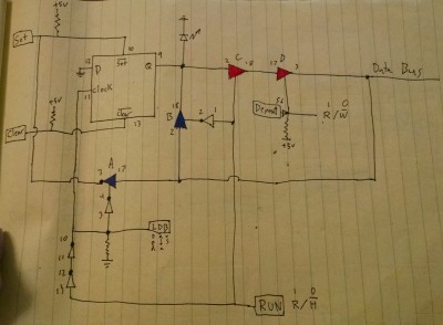
IMG_20180313_012217271.jpg [ 1.69 MiB | Viewed 6842 times ]
Data Control Card
Here we see the fundamental element of the data control card which is far more complicated than it needs to be. This has to be like revision 6 by now. There are effectively 8 of these, one per byte. Thus, there are 8 D-latches acting as RS flip-flops (7474's), and 8 of each tri-state buffer (3x 74244, 1x 74240). The inverters that control the buffers are not duplicated.

The idea is that we can load a value from the data bus into these D-latches. The load signal clears the flip-flop, and then lets any 1's populate their respective flop-flops. Say you made a mistake, and need to change a single bit, you use the set/clear momentary switches to make your changes. This will be visible on the LEDs, while not interfering with the data bus. When you are happy with the value, you can deposit it right back onto the data bus by twiddling the R/W line to make RAM overwrite the new value.

However, all of that is rendered dormant while the CPU is running. One buffer prevents this card from interfering with the data bus. while another buffer now allows the LEDs to directly view data bus activity. The flip-flops are cleared whenever the CPU is running.

Attachment:
File comment: Data Control Rev 8
IMG_20180319_203629161_HDR.jpg
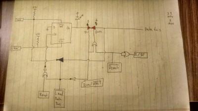
IMG_20180319_203629161_HDR.jpg [ 4.11 MiB | Viewed 6842 times ]

I've managed to simplify the design a bit since this point for revision 8, but I'm holding off on building the improved version for the moment. Every time I think I've reduced the complexity on this card (while retaining the same functionality), someone consistently points out a new way for me to improve it (which I should note is more than welcome). Rev 8 doesn't reduce the chip count all that much, but it does reduce the total gates to 29, and eliminates quite a few wires, which makes me happy. I wish I had understood the 74245 sooner.

Attachment:
File comment: Address Control
IMG_20180411_051334891.jpg
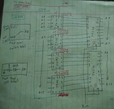
IMG_20180411_051334891.jpg [ 1.7 MiB | Viewed 6842 times ]
Address Control Card
This one is probably the most straight-forward card in the bunch. Want to hop to a specific address? Set the toggle switches, and load up that address. Then, you can increment from there to see what is in subsequent addresses. Again, this card has a run lockout to prevent interference when the CPU should be in control of the address bus. The LEDs here are always watching the address bus. Upon typing this, 8 months after assembling the card, I realize I should probably add buffers to prevent extending the address bus lines unnecessarily...

Attachment:
File comment: Status Control
IMG_20180305_062126442.png
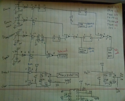
IMG_20180305_062126442.png [ 5.53 MiB | Viewed 6842 times ]
Status Control Card
The status control card feels like a mess to me. It's been revised slightly since this schematic was laid down, but the fundamentals still apply, so for the moment it will do. The job of status control is to pass signals to the data and address cards, letting them know when to Deposit, load the data bus, load the address bus, and increment an address. It also controls weather the CPU is running or halted, as well as if memory is protected (not that this feature works right now). This card became a catch-all for the switches not specific to the data or address cards.

The Examine, Examine Next, Deposit, and Deposit Next momentary switches are all debounced using a simple RC circuit and inverting Schmitt triggers. I only have a cursory understanding of this circuit, as it was suggested to me a few months ago by a friend. Memory Protect, Protect Clear, Halt, and Run instead have toggles, and so I did not include debouncing circuitry. The Step momentary could do with a debounce circuit, but Reset has a DS1233 for the CPU to let it reset cleanly so I'm not worried about it right now.

The complex portion of handling status control is orchestrating the sequence of events needed for things like Examine, Examine Next, and Deposit Next to work right. The timing of these events is determined by a 555 timer and daisy chained D latches that are supposed to ripple down the chain in order. Now that I have a logic analyzer, I want to watch this process happen, step by step.

  • Examine tells the address card to load whatever address is on the toggle switches, then tells the data card to load whatever is on the data bus value into the front panel registers to be viewed on the LED indicators. [Load Address] -> [Load Data Bus]
  • Examine Next doesn't load from the toggle switches, but instead tells the address card to increment the counters on the address control card, followed by loading the data bus for viewing. [Increment Address] -> [Load Data Bus]
  • Deposit Next is the most complicated one. First, the data value on the front panel is written to the data bus, then the address is incremented, then the data bus value at this new address is loaded into the front panel's registers. [Deposit] -> [Increment Address] -> [Load Data Bus]
  • Deposit is simple, and doesn't abide by the sequencing, allowing you to directly write a value from the front panel into RAM.

My understanding is that I'm performing Deposit Next backwards compared to an Altair 8800. Whereas the 8800 deposits that value into the location after the one you are currently viewing, mine deposits it into the current address you're viewing, then increments the address to show the value in there. This way if you're re-entering in data and don't wish to overwrite the value at that address, you can press Examine Next instead, and move on. Made a mistake, but only want to change a bit or two of that value, rather than all 8? You can do that too.

I hope I'm explaining this well enough. Feel free to ask whatever questions come to mind.

_________________
The Cactus


Top
 Profile  
Reply with quote  
PostPosted: Wed Apr 11, 2018 12:29 pm 
Offline
User avatar

Joined: Tue Apr 03, 2018 2:10 pm
Posts: 125
Thanks for sharing all that. I wasn't familiar with the 74xx193 - which is exactly what I've been looking for. I'm probably going to do a different set of switches, maybe a bit simpler. I just want blinkenlights and play value. I started off looking at the Altair (I have the Altair-Duino kit) and the PDP-8 (yup, I have the PiDP kit) and I think my solution will end up somewhere between the two.

It had also occurred to be to try to implement some kind of general-purpose front panel that could be used as a control surface for a number of projects.

I'll be studying your schematics carefully!

_________________
I like it when things smoke.
BlogZolatron 64 project


Top
 Profile  
Reply with quote  
PostPosted: Thu Apr 12, 2018 7:41 am 
Offline
User avatar

Joined: Tue Apr 03, 2018 2:10 pm
Posts: 125
CommodoreZ wrote:
switches are all debounced using a simple RC circuit and inverting Schmitt triggers.


Coincidentally, I have been looking into the same thing. I did a post about it - mainly because I wanted to play with my oscilloscope.

_________________
I like it when things smoke.
BlogZolatron 64 project


Top
 Profile  
Reply with quote  
PostPosted: Thu Apr 12, 2018 10:24 am 
Offline
User avatar

Joined: Mon Apr 09, 2018 11:33 am
Posts: 19
Location: Free Country, USA
It took awhile to select the 74193 as the right sort of 4-bit binary counter. There are quite a few options, but this one had the features I needed for cascading together and loading a value. My schematics are admittedly dubious. Until I have something 100% working, I wouldn't trust my work as any sort of guideline.

Right now I'm selecting matching electrolytic capacitors to sit on each card's power rail to hopefully combat power dips. I'm thinking 47μF caps right now.

Here's a closeup of the bus itself.
Attachment:
IMG_20150501_012712638.jpg
IMG_20150501_012712638.jpg [ 4.34 MiB | Viewed 6764 times ]


I intend to do a hard-wired NOP test soon after adding those electrolytic capacitors, but I'm not entirely sure what I should be looking for other than the address bus jumping around.

_________________
The Cactus


Top
 Profile  
Reply with quote  
PostPosted: Thu Apr 12, 2018 3:35 pm 
Offline
User avatar

Joined: Thu Dec 11, 2008 1:28 pm
Posts: 10793
Location: England
If a computer doesn't work, there are a myriad of things which might be wrong, so the point of experiment is to try to narrow down what needs fixing.

For a NOP test to work, you need a working CPU, a good power supply and clock, and the various CPU lines tied off in the right way. If you can observe the address bus closely you can rule out shorts, opens, or unwanted reorderings. To a small degree you've also shown the data bus is OK. If you do the NOP tie off a long way from the CPU, you might be showing something about your motherboard or backplane too. As there are various values which can serve as a NOP test you can take it a little further, showing the databus is working as intended.

After the NOP test you might put a tight loop into a ROM and try running that, to show that the ROM is correctly wired up, correctly accessed and correctly programmed.

Then you can run something with JSR and RTS and show that RAM is working.

And so on.


Top
 Profile  
Reply with quote  
Display posts from previous:  Sort by  
Post new topic Reply to topic  [ 47 posts ]  Go to page 1, 2, 3, 4  Next

All times are UTC


Who is online

Users browsing this forum: No registered users and 28 guests


You cannot post new topics in this forum
You cannot reply to topics in this forum
You cannot edit your posts in this forum
You cannot delete your posts in this forum
You cannot post attachments in this forum

Search for:
Jump to: