6502.org Forum  Projects  Code  Documents  Tools  Forum
It is currently Sun Apr 28, 2024 6:49 pm

All times are UTC


Post new topic Reply to topic  [ 34 posts ]  Go to page Previous  1, 2, 3
Author Message
PostPosted: Thu Feb 25, 2016 6:22 am 
Offline
User avatar

Joined: Fri Aug 30, 2002 1:09 am
Posts: 8428
Location: Southern California
Avoiding bus contention if you were to accidentally write to an EPROM address, with a minimum of parts, seems to be the main focus on this one. I would say however that such writes are not really a concern. The program-bug conditions that would make them happen will be rare and probably be encountered only during program development and then fixed, and be at too low of a duty cycle to cause any hardware damage, and the bug would probably make your program crash anyway even with the hardware protection against writing to EPROM.

cbmeeks is only going for 2MHz max here though, so there's not really any need to select the EPROM before phase 2 and get all the access time that becomes available that way unless the EPROMs are antiques of 250ns or slower. :lol: EPROMs will produce the first roadblock as you turn the clock rate up though.

_________________
http://WilsonMinesCo.com/ lots of 6502 resources
The "second front page" is http://wilsonminesco.com/links.html .
What's an additional VIA among friends, anyhow?


Top
 Profile  
Reply with quote  
PostPosted: Thu Feb 25, 2016 8:52 am 
Offline
User avatar

Joined: Wed Feb 13, 2013 1:38 pm
Posts: 586
Location: Michigan, USA
BigDumbDinosaur wrote:
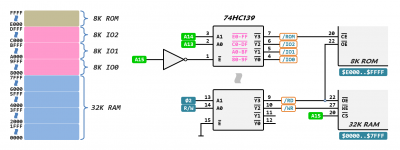
Also, the simultaneous assertion of /CE and /OE on the EPROM will have some negative effects on performance.

It's best if /CE is asserted as soon as the address bus goes valid with an EPROM address, even though Ø2 is still low. /OE should only be asserted when Ø2 goes high. Controlling both inputs from a single source, as shown in the above circuit, narrows the window of opportunity to read the EPROM before the end of the bus cycle. This because it takes time for the EPROM to come out of the high-Z state and connect to the bus, which can only occur when both /CE and /OE have been asserted. Asserting /CE is what "wakes up" the device from low power mode and typically takes the most time. Hence the suggestion that /CE be asserted as soon as a valid address exists. Reading the device should be gated only with /OE.

Perhaps the circuit could be modified to assert the ROM chip enable, like so;
Attachment:
Beattie Notes.png
Beattie Notes.png [ 85.97 KiB | Viewed 161 times ]

Does anyone know by how much PHI1 leads PHI2, please? I'm not sure I understand the timing diagrams in the Datasheets.

TIA... Mike


Last edited by Michael on Thu Jul 08, 2021 5:21 am, edited 2 times in total.

Top
 Profile  
Reply with quote  
PostPosted: Tue Mar 01, 2016 8:28 pm 
Offline
User avatar

Joined: Fri Aug 30, 2002 1:09 am
Posts: 8428
Location: Southern California
Michael wrote:
Does anyone know by how much PHI1 leads PHI2, please? I'm not sure I understand the timing diagrams in the Datasheets.

WDC no longer guarantees or measures the delays between Φ0 (ie Φ2 in), Φ1, and Φ2 (ie Φ2 out), and they don't recommend using Φ1 or Φ2 out. I think that's silly, since the circuits are still there and they work and yes you can hang an RC or a crystal on the processor itself and it will still work; but since they don't guarantee it, we're on our own if we do it. If they don't recommend using them, they could use those pins for something else useful. Anyway, I looked at an older data sheet and saw that the guaranteed max delay between Φ0 and Φ1, and also the guaranteed max delay between Φ0 and Φ2, for the 14MHz W65c02S, was 22ns. It's strange that they would have the same number for both, as I think that internally Φ2 (out) is derived by running Φ1 into an inverter and then using its output for Φ2 (out).

_________________
http://WilsonMinesCo.com/ lots of 6502 resources
The "second front page" is http://wilsonminesco.com/links.html .
What's an additional VIA among friends, anyhow?


Top
 Profile  
Reply with quote  
PostPosted: Wed Mar 02, 2016 6:25 am 
Offline
User avatar

Joined: Thu May 28, 2009 9:46 pm
Posts: 8151
Location: Midwestern USA
Michael wrote:
Does anyone know by how much PHI1 leads PHI2, please? I'm not sure I understand the timing diagrams in the Datasheets.

The clock outputs on the 65C02 are there to facilitate the retrofit of the 'C02 to systems that used the NMOS 6502. As Garth noted, WDC does not (and has not for a long time) tested the timing characteristics of the clock outputs of their 65C02 production parts. Use of those outputs is not recommended in new designs.

Note that the 65C816 does not have clock outputs—only a clock input exists. If you are designing something in which you eventually may want to install the 65C816 and need a two-phase clock you'll have to roll your own. The below circuit uses a TTL can oscillator and one section of a 74ABT74 flip-flop to produce a two-phase clock with a very sharp rise and fall and no lead or lag between outputs.

Attachment:
File comment: Two-Phase Clock Generator
clock_gen_2p.gif
clock_gen_2p.gif [ 53.85 KiB | Viewed 754 times ]

_________________
x86?  We ain't got no x86.  We don't NEED no stinking x86!


Top
 Profile  
Reply with quote  
Display posts from previous:  Sort by  
Post new topic Reply to topic  [ 34 posts ]  Go to page Previous  1, 2, 3

All times are UTC


Who is online

Users browsing this forum: No registered users and 7 guests


You cannot post new topics in this forum
You cannot reply to topics in this forum
You cannot edit your posts in this forum
You cannot delete your posts in this forum
You cannot post attachments in this forum

Search for:
Jump to: