6502.org Forum  Projects  Code  Documents  Tools  Forum
It is currently Fri Oct 18, 2024 1:17 pm

All times are UTC


Post new topic Reply to topic  [ 9 posts ] 
Author Message
 Post subject: Timing diagram question
PostPosted: Wed Jun 03, 2015 6:30 am 
Offline
User avatar

Joined: Tue Feb 10, 2015 5:27 pm
Posts: 80
Location: Germany
The 6509 datasheet shows TACC starting at the rising phase of phi2 - this should be an error for TACC>phi2 and the corresponding 6502 diagrams show TACC starting at the beginning of address setup?


Going from there to see if I'm correct:

Can I simply take TACC from the datasheet and this is the time I have for memory access time plus propagation delays?
Or do I have to calculate:
Cycle time (500ns @2MHz) - TADS (150ns) - TDSU (50ns - Data Stability Time - is that the correct value??) => Access time 300ns (which coincides with TACC).

So a 150ns RAM would leave me with comfortable 150ns for glue logic?


Top
 Profile  
Reply with quote  
PostPosted: Wed Jun 03, 2015 8:12 am 
Offline
User avatar

Joined: Thu Dec 11, 2008 1:28 pm
Posts: 10961
Location: England
Bad datasheet! I think TACC has no place on that timing diagram. What the MPU cares about is TDSU.

Datasheet: http://archive.6502.org/datasheets/mos_6509_mpu.pdf


Attachments:
MOS6509-read-timing.png
MOS6509-read-timing.png [ 115.68 KiB | Viewed 1577 times ]
Top
 Profile  
Reply with quote  
PostPosted: Wed Jun 03, 2015 8:43 am 
Offline
User avatar

Joined: Tue Feb 10, 2015 5:27 pm
Posts: 80
Location: Germany
Yes, that was/is the diagram I'm looking on...


Is my calculation above right?
And in case of e.g. a 6522 VIA (@2MHz), which needs address being setup 90ns before phi2 rising, that leaves me with only phi1(215ns)-TADS-90ns(VIA)=35ns for glue logic? =:-O


Top
 Profile  
Reply with quote  
PostPosted: Fri Jun 05, 2015 4:33 am 
Offline
User avatar

Joined: Fri Dec 11, 2009 3:50 pm
Posts: 3367
Location: Ontario, Canada
Hobbit1972 wrote:
The 6509 datasheet shows TACC starting at the rising phase of phi2 - this should be an error for TACC>phi2 and the corresponding 6502 diagrams show TACC starting at the beginning of address setup?
Yes -- it seems clear there's an error in the diagram. The Memory Read Access time (TACC) begins when the address becomes stable.


Attachments:
MOS6509-read-timing revised.png
MOS6509-read-timing revised.png [ 105.17 KiB | Viewed 1529 times ]

_________________
In 1988 my 65C02 got six new registers and 44 new full-speed instructions!
https://laughtonelectronics.com/Arcana/ ... mmary.html
Top
 Profile  
Reply with quote  
PostPosted: Fri Jun 05, 2015 5:40 am 
Offline
User avatar

Joined: Tue Feb 10, 2015 5:27 pm
Posts: 80
Location: Germany
Err... I slightly miscalculated above...

At 2MHz, it is
phi1 (min) 215ns
TADS (max) 150ns
VIA must have valid address 90ns before rising of phi2

phi1-TADS = 65ns --- which is far below the required 90ns. :?:
Even throwing in the fall time of phi1 won't change much.


Do I have a flaw in the maths/figures or are those numbers of the datasheet misleading? (Because there are a lot of systems out there with a VIA working.) :?:


Top
 Profile  
Reply with quote  
PostPosted: Sun Jun 07, 2015 12:12 am 
Offline
User avatar

Joined: Fri Dec 11, 2009 3:50 pm
Posts: 3367
Location: Ontario, Canada
Here's a simplistic but useful summary. At 2 MHz the cycle time will be 500 ns, by which I mean 250 ns of Phase1 and 250 ns of Phase2 (see post-script below). That assumes the rise and fall times on the Φ1 and Φ2 inputs are zero -- which is only a slight inaccuracy. Looking at the 6509 datasheet AC Characteristics, we see 150 ns listed as the maximum tADS delay for 2 MHz operation. IOW, the address lines will be valid 150 ns (or less) after the start of Phase1. The address lines will be stable during the remaining 100 ns of Phase1 -- ie, valid 100ns (or more) before Phase2 starts.

I don't know which 6522 datasheet you're referring to -- many different manufacturers source 6522s -- but it sounds as if the pertinent device may not be fast enough for guaranteed operation within this roughly-calculated 100 ns margin. It may (and probably will) work, but operation can't be guaranteed (due to variations in manufacturing process, supply voltage and temperature). If your 6522 needs the register select inputs valid 90 ns before the start of Phase2 then that issue will be OK, given that the RS inputs typically connect directly from the CPU address outputs. But if 90 ns is also the specified setup for CS and /CS then you have a problem, since you'll have some address-decode logic that must process the address before outputting a chip-select signal to the 6522. Your options include slowing the CPU clock or selecting a faster-rated 6522 even though you plan to run it at only 2 MHz. What matters is satisfying its spec for setup time etc.

Getting back to the 6509, I notice that, unlike 6502 and 'C02, it requires 6800-style clocking -- ie; two non-overlapping clock signals, with virtually rail-to-rail voltage swings. :!: For a 6800/6509 clock generator circuit I'd suggest using a fast CMOS family such as 74AC. This'll avoid sluggish rise & fall times which waste some of the cycle time.

Does anyone know of a better version of the 6509 datasheet? This one is terrible! I noticed several more errors, such as the absurd memory map, and the fact the timing diagram for writes repeatedly details a clock-low voltage as 2.0V rather than 0.2V. Also, the datasheet lists 1 MHz, 2 MHz and 3 MHz timing figures, implying that three different speed grades were available. But nowhere do I see a part-number scheme (such as -1, -2 and -3 or -A -B and -C suffixes).

ps- the datasheet also lists differing spec's for minimum Phase1 pulse width (215 ns) and minimum Phase2 pulse width (235 ns) for a 2 MHz device. It's odd that they're asymmetrical, and that the numbers are so low (they suggest operation faster than 2 MHz). Assuming that's not just another boo-boo then that alters the 6522 setup-time issue substantially -- but only if you're operating at 215 and 235 ns. There's no need to do that. Phase1 and Phase2 can be 240 ns each, even if each is bracketed with 5 ns for rise time and 5 ns for fall time.

-- Jeff

_________________
In 1988 my 65C02 got six new registers and 44 new full-speed instructions!
https://laughtonelectronics.com/Arcana/ ... mmary.html


Top
 Profile  
Reply with quote  
PostPosted: Sun Jun 07, 2015 8:02 am 
Offline
User avatar

Joined: Tue Feb 10, 2015 5:27 pm
Posts: 80
Location: Germany
Thank you Garth and Jeff for seeing me through!

The major flaw in my calculation was taking 215ns from the datasheet and not the 250ns my clock circuit actually produces.


Dr Jefyll wrote:
I don't know which 6522 datasheet you're referring to

Datasheet MOS VIA 1977 from 6502 archive, and of MOS 6551 ACIA also from there. For now I only possess the ACIA, but the datasheet speaks of the same timing requirement of 90ns.


Dr Jefyll wrote:
-- many different manufacturers source 6522s -- but it sounds as if the pertinent device may not be fast enough for guaranteed operation within this roughly-calculated 100 ns margin. It may (and probably will) work, but operation can't be guaranteed (due to variations in manufacturing process, supply voltage and temperature). If your 6522 needs the register select inputs valid 90 ns before the start of Phase2 then that issue will be OK, given that the RS inputs typically connect directly from the CPU address outputs. But if 90 ns is also the specified setup for CS and /CS then you have a problem, since you'll have some address-decode logic that must process the address before outputting a chip-select signal to the 6522. Your options include slowing the CPU clock or selecting a faster-rated 6522 even though you plan to run it at only 2 MHz. What matters is satisfying its spec for setup time etc.


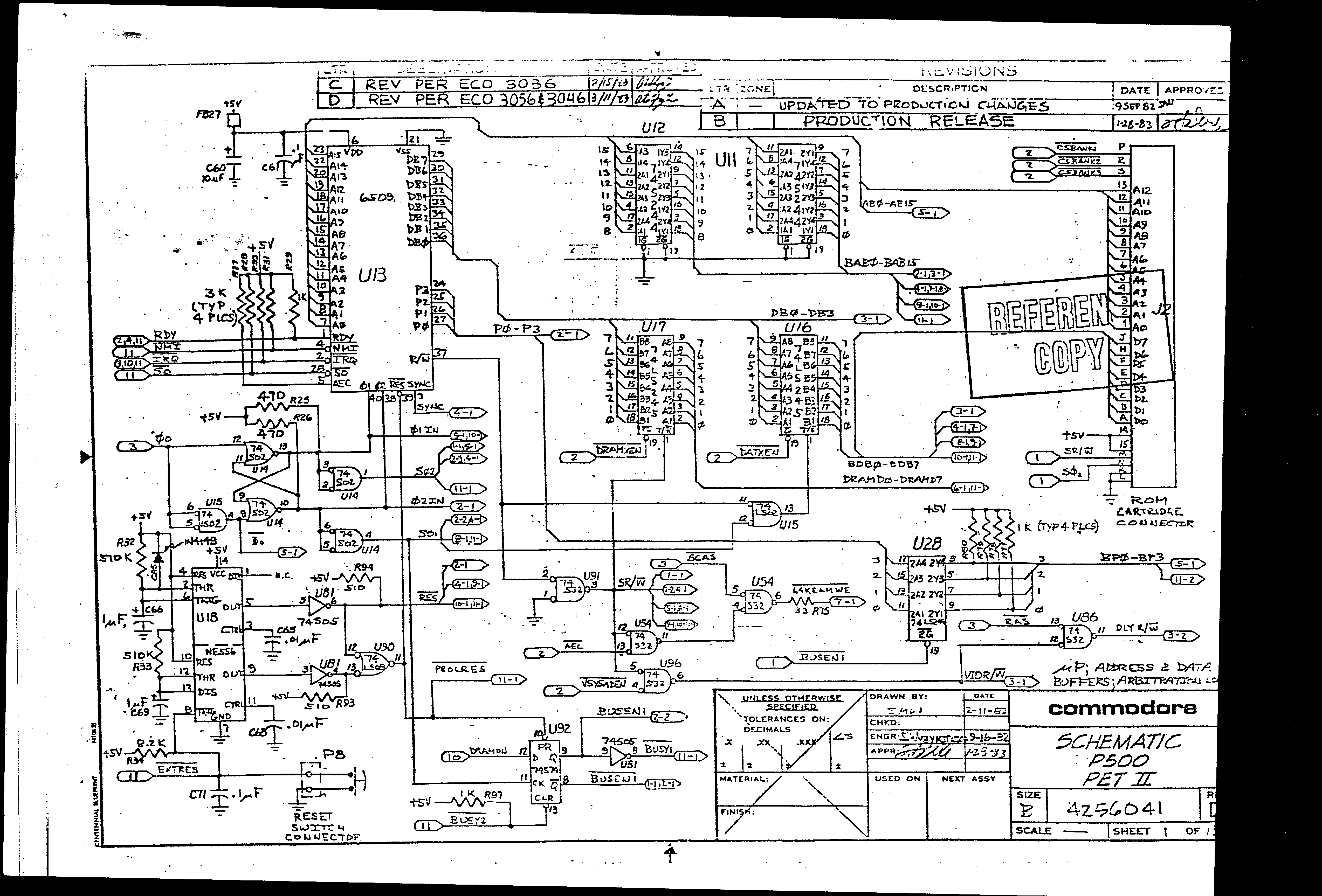
Let's see how they do it in CBM 610 - 6509 & 6551 running at 2MHz system speed. (Why didn't I have that idea earlier??) http://www.6502.org/users/sjgray/computer/cbm2/cbm2-schematics-8256043-bl.pdf
ACIA-CS comes out of 74S138 which depends on another 74S138 which in turn depends on a 74S241 line driver. ACIA-phi2 seems to be the undelayed phi2.
*woops* - to me it looks like
phi1 250ns - TACC 150ns => 100 ns time left
ACIA datasheet says address must be valid 90ns before rise of phi2 - that would leave only 10ns for glue logic :mrgreen:
My 138 datasheet lists a typical delay of 18-27ns, so that is at least 54ns (and not taking into account delay in '241) => 46ns left for ACIA instead of 90ns.
(Maximum specs are 27-40ns - in those areas not much of the 100ns would be left...)

If your theory is right, and ACIA only needs RS-lines valid that early, even then the construction is hardly within spec. (Good that reality seldom knows about specs...)


What do I learn from this? MOS specs are bogus? MOS specs are a raw estimates and used only for preliminary orientation? ;)


Dr Jefyll wrote:
Getting back to the 6509, I notice that, unlike 6502 and 'C02, it requires 6800-style clocking -- ie; two non-overlapping clock signals, with virtually rail-to-rail voltage swings. :!: For a 6800/6509 clock generator circuit I'd suggest using a fast CMOS family such as 74AC. This'll avoid sluggish rise & fall times which waste some of the cycle time.

For clock generation I copied the circuit of CBM 500 http://www.commodore.ca/manuals/funet/cbm/schematics/computers/p500/4256041-01of15.gif using LS02ALS. Which seems to work so far. (Don't ask me about the looks of rise and fall - no oscilloscope here.)

But that brings me to another question - but that rather should go to nostalgia: why did MOS drop/not use the clock generation inside 6502 using only one input clock? I can't imagine that they needed the die space so badly, and I can't imagine either what application would make it necessary to have it that way.


Dr Jefyll wrote:
Does anyone know of a better version of the 6509 datasheet? This one is terrible! I noticed several more errors, such as the absurd memory map, and the fact the timing diagram for writes repeatedly details a clock-low voltage as 2.0V rather than 0.2V. Also, the datasheet lists 1 MHz, 2 MHz and 3 MHz timing figures, implying that three different speed grades were available. But nowhere do I see a part-number scheme (such as -1, -2 and -3 or -A -B and -C suffixes).

I only have seen the one here in the archive. (But I didn't search for another one so far to be honest.)
(The part number scheme should be the one MOS used throughout all its 65xx parts: no appendix: 1MHz, A 2MHz, B 3MHz, C 4MHz).


Top
 Profile  
Reply with quote  
PostPosted: Sun Jun 07, 2015 9:35 am 
Offline
User avatar

Joined: Thu Dec 11, 2008 1:28 pm
Posts: 10961
Location: England
Hobbit1972 wrote:
why did MOS drop/not use the clock generation inside 6502 using only one input clock? I can't imagine that they needed the die space so badly, and I can't imagine either what application would make it necessary to have it that way.

It does seem odd. As you say, it clears up some space at the top edge of the die - in fact with the AEC control, it looks like it's the 6501 masks they used as a basis. But the top edge isn't a good place to detect address zero - that would be the bottom edge. We need to take some die photos!
Perhaps for some reason it was easy for Commodore to provide non-overlapping clocks in their application.


Top
 Profile  
Reply with quote  
PostPosted: Sun Jun 07, 2015 9:52 am 
Offline
User avatar

Joined: Tue Feb 10, 2015 5:27 pm
Posts: 80
Location: Germany
BigEd wrote:
Hobbit1972 wrote:
why did MOS drop/not use the clock generation inside 6502 using only one input clock? I can't imagine that they needed the die space so badly, and I can't imagine either what application would make it necessary to have it that way.

It does seem odd. As you say, it clears up some space at the top edge of the die - in fact with the AEC control, it looks like it's the 6501 masks they used as a basis. But the top edge isn't a good place to detect address zero - that would be the bottom edge. We need to take some die photos!
Perhaps for some reason it was easy for Commodore to provide non-overlapping clocks in their application.


As 6509 AFAIK was only used in CBM 500/600 the non-overlapping clock is "easy" for it only requires one LS02 to generate, but it would have been easier without that extra chip. Are there any applications known where phi1 and phi2 are not only inverted to each other but effectively have different duty cycles?

To make things more confusing: 6510 has clock generating logic on board, phi1 in and phi2 out, 6501-1 is like 6509: phi1+phi2 in, 6502-2 has phi2 in and phi2 out - though I never heard of both chips (-1/-2) outside this datasheet... as a rough guess that seems to indicate that the same clock circuit would be present in all variants and just the bonding different.

Looking at those variants: 6501-1 and -2 sacrifice RDY to have an extra port pin. But what use is having AEC without RDY?


Top
 Profile  
Reply with quote  
Display posts from previous:  Sort by  
Post new topic Reply to topic  [ 9 posts ] 

All times are UTC


Who is online

Users browsing this forum: No registered users and 6 guests


You cannot post new topics in this forum
You cannot reply to topics in this forum
You cannot edit your posts in this forum
You cannot delete your posts in this forum
You cannot post attachments in this forum

Search for:
Jump to: