6502.org Forum  Projects  Code  Documents  Tools  Forum
It is currently Sun May 05, 2024 8:52 am

All times are UTC


Post new topic Reply to topic  [ 54 posts ]  Go to page 1, 2, 3, 4  Next
Author Message
PostPosted: Tue Mar 17, 2015 2:08 am 
Offline

Joined: Wed Feb 05, 2014 7:02 pm
Posts: 158
I think the First Steps phase has at last ended after a year. Though I didn't have much to show for it, I still learned some valuable lessons from having my ideas (constructively) scrutinized. I think the most important thing I learned, even though it's emphasized over and over and over on this site is: My initial goals were too much and that I needed to make tradeoffs. I wish I could put everything and the kitchen sink onto my SBC, and make it all discrete logic/building-friendly, but without PALs/CPLDs/level shifters and friends, I can only do so much.

I scaled back my project to the following goals:
  1. Use 65816 processor. Consider a 6502 build later.
  2. Just get something working first. Worry about ISA interfacing later (R1). This will be R0.
  3. Design for theoretical operation at at least 10MHz. Higher is better. 14MHz may be possible (I'll discuss later).
  4. Use parts that are still made.
  5. Use discrete components and TTL glue logic (I think I found a setup where 14MHz operation is possible with discrete TTL).
  6. Bank 0 should be distinguished, so that other banks can be used for extra RAM.

The plan is to build for 8MHz on veroboard using soldering (I have no provisions for wire wrap right now) or maybe lower speed- depends what TTL parts I have on hand. For theoretical operation, I've went through the trouble of calculating propogation delays, and trying to reduce the delays for the slowest parts (EPROM). To that end, I am using the linked Python program. The Python program's variables should be self-explanatory, but it attempts to calculate the propagation delay from PHI2's falling edge to the time the EPROM is selected, and returns the maximum access time that satisfies the circuit so that data is out 10ns before PHI2's falling edge.

Memory Map is as follows (ROM split is deliberate- it's not important why, so don't ask):
|0x0000-0x3FFF|RAM|
|0x4000-0x7FFF|PRG ROM (Extra Forth words, helper routines, etc)|
|0x8000-0xBFFF|IO (VIA, ACIA, maybe PIA in future)|
|0xC000-0xFFFF|SYSTEM ROM|
|0x10000+|Extra RAM/ROM (future expansion)|

The program/schematic makes the following assumptions
  1. RWB is NOT gated for EPROM access (so attempt to write to ROM addresses will cause contention).
  2. BA0-7 to 373 setup time is not violated (it is neglible for ACT/ABT anyway).
  3. Delay from 373 output to Output Enable is longer than VDA/VPA to Output Enable.

The parts I used are the following (some are available in ABT variants), taken from search datasheets on Mouser:

|Connection |TTL Chip |Prop Delay (ns)|
|:------------------|:--------- |:--------------|
|BA0-7 to A16-23 |74ACT373N |10.4|
|BA0-7 to D0-7 |74ACT245N |9|
|A16-23 to BANK_ZERO|74ACT11030|8.1|
|Many |SN74ACT00N |8.5|

And lastly, I have attached the schematic of my current setup for EPROM accesses. First image is the CPU sheet, second is the EPROM and RAM sheet (ignore the RAM portion- it is wrong). The circuit below satisfies the A16-23 to ~OE conditions from my program for 8MHz, since:
8.1ns (8-input NAND) + 8.5ns (NAND) is < 33.6 ns.
VDA/VPA is also satisfied, as relative to PHI2's falling edge,
30ns address setup + 10ns data setup + 17ns OR (two NANDs) + 8.5ns = 65.5ns, which is less than 125ns-15ns = 115 ns for 8 MHz. I'll add that to my program later.

Code:
F:\Legacy\6502\SOURCE\R1\src>r1timing.py
Desired 65816 frequency (MHz): 8
Decoding delay from A0-A15 to ~CE (ns): 8.5
Required EPROM speed w/ 8.5 glue logic (max access time): 76.5
Decoding delay from A16-23 to ~OE: 33.6
Required bank 0x1-0xFF RAM/EPROM speed w/o glue logic: 33.6


CPU sheet:
Attachment:
r1_cpu.png
r1_cpu.png [ 211.47 KiB | Viewed 1482 times ]


EPROM glue sheet:
Attachment:
r1_eprom.PNG
r1_eprom.PNG [ 157.98 KiB | Viewed 1482 times ]


Does anyone who has dealt with higher speeds think I'm on the right track?


Last edited by cr1901 on Tue Mar 17, 2015 4:23 am, edited 1 time in total.

Top
 Profile  
Reply with quote  
PostPosted: Tue Mar 17, 2015 2:29 am 
Offline

Joined: Wed Feb 05, 2014 7:02 pm
Posts: 158
EDIT: Ignore the below text. I re-uploaded the corrected schematics as attachments.

The BUS_VALID control signal is wrong. I intended to implement an OR gate, but as I just remembered, that's not how one does it using NAND gates (http://en.wikipedia.org/wiki/NAND_logic#OR) :P. Doesn't change the propagation delay, but it will confuse anyone looking at the circuit.


Top
 Profile  
Reply with quote  
PostPosted: Tue Mar 17, 2015 5:08 am 
Offline
User avatar

Joined: Thu May 28, 2009 9:46 pm
Posts: 8173
Location: Midwestern USA
I'd use 74AC instead of 74ACT, as many 74ACT devices are slower than their 74AC counterparts. Also, if you are using only CMOS devices 74xCT logic does nothing for you.

_________________
x86?  We ain't got no x86.  We don't NEED no stinking x86!


Top
 Profile  
Reply with quote  
PostPosted: Tue Mar 17, 2015 5:30 am 
Offline

Joined: Wed Feb 05, 2014 7:02 pm
Posts: 158
BigDumbDinosaur wrote:
I'd use 74AC instead of 74ACT, as many 74ACT devices are slower than their 74AC counterparts. Also, if you are using only CMOS devices 74xCT logic does nothing for you.
I thought the "T" meant TTL voltage levels? And I'm not sure if I'm using purely CMOS devices or not. The WDC devices themselves, of course, are CMOS. I may need to eventually interface to a TTL voltage-only bus, or peripheral, so I guess I could use a hybrid of AC and ACT families?

I'm also interested in knowing whether I missed anything or my circuit works as intended? I.e. it will access EPROM- prepare the outputs- only when A14 is asserted, and will actually enable the output when the circuit knows a Bank 0 access is intended and VDA/VPA indicate the bus is valid. I qualified ~OE with VPA OR VDA (made of NANDs), so I think I'm good there.


Top
 Profile  
Reply with quote  
PostPosted: Tue Mar 17, 2015 6:41 am 
Offline
User avatar

Joined: Fri Aug 30, 2002 1:09 am
Posts: 8432
Location: Southern California
cr1901 wrote:
BigDumbDinosaur wrote:
I'd use 74AC instead of 74ACT, as many 74ACT devices are slower than their 74AC counterparts. Also, if you are using only CMOS devices 74xCT logic does nothing for you.
I thought the "T" meant TTL voltage levels? And I'm not sure if I'm using purely CMOS devices or not. The WDC devices themselves, of course, are CMOS. I may need to eventually interface to a TTL voltage-only bus, or peripheral, so I guess I could use a hybrid of AC and ACT families?

CMOS can drive the bipolar logic like LS, as it can pull all the way to ground and all the way to Vcc. Bipolar logic like LS don't do as well at driving CMOS (like 74AC), as it cannot pull up high enough to really totally guarantee valid logic 1's. Hence the CMOS ones with the "T" in them, like 74HCT and 74ACT. These latter two are more universal. Their input thresholds match up to bipolar logic's, and their output go all the way to the rails so they can drive either type. TTL however presents heavier loads at the inputs than CMOS, and CMOS definitely has the advantage in power consumption and usually speed as well. I never use 74LS unless I need it right now, late at night, and it's all I have, and I can't get a CMOS part here for another day or a few days. I've pushed my luck with LS, and so far, in the few times I've used it temporarily, it has worked, but I put the CMOS part in when it arrives.

Quote:
I'm also interested in knowing whether I missed anything or my circuit works as intended?

If I'm looking at it straight:
  • It looks like OE\ and T/R\ on U2 need to be swapped.
  • U10.1 needs to be an NOR gate, not NAND. If any one or another of the inputs goes up, you want the output to go down. You want the output to be high only if all the inputs are low.

_________________
http://WilsonMinesCo.com/ lots of 6502 resources
The "second front page" is http://wilsonminesco.com/links.html .
What's an additional VIA among friends, anyhow?


Top
 Profile  
Reply with quote  
PostPosted: Tue Mar 17, 2015 6:48 am 
Offline
User avatar

Joined: Thu May 28, 2009 9:46 pm
Posts: 8173
Location: Midwestern USA
cr1901 wrote:
I'm also interested in knowing whether I missed anything or my circuit works as intended?

I tried to look at it but must be missing some aspects due to color usage. I tried display it as grey-scale but that was actually worse.

_________________
x86?  We ain't got no x86.  We don't NEED no stinking x86!


Top
 Profile  
Reply with quote  
PostPosted: Tue Mar 17, 2015 7:50 am 
Offline

Joined: Wed Feb 05, 2014 7:02 pm
Posts: 158
GARTHWILSON wrote:
If I'm looking at it straight:
  • It looks like OE\ and T/R\ on U2 need to be swapped.
  • U10.1 needs to be an NOR gate, not NAND. If any one or another of the inputs goes up, you want the output to go down. You want the output to be high only if all the inputs are low.

Correct on both accounts! The NAND is only low for all ones. This is exactly why I wanted a second/third/fourth pair of eyes :P. I can't logic well.

It appears that 8-input NORs, however, are more difficult to find.


Top
 Profile  
Reply with quote  
PostPosted: Tue Mar 17, 2015 8:58 am 
Offline

Joined: Sun Apr 10, 2011 8:29 am
Posts: 597
Location: Norway/Japan
BigDumbDinosaur wrote:
cr1901 wrote:
I'm also interested in knowing whether I missed anything or my circuit works as intended?

I tried to look at it but must be missing some aspects due to color usage. I tried display it as grey-scale but that was actually worse.
I have to agree with BDD here.. I can see the colours, but it's not enhancing the view. Good old schematics on a white background is far easier to read and check. The dark theme is very hard to look at.

-Tor


Top
 Profile  
Reply with quote  
PostPosted: Tue Mar 17, 2015 9:24 am 
Offline

Joined: Wed Feb 05, 2014 7:02 pm
Posts: 158
*Grumbles about DipTrace's poor presentation choices* Nothing has been changed from previous schematic except color scheme, errors and all.


Attachments:
r1_eprom_w.PNG
r1_eprom_w.PNG [ 168.86 KiB | Viewed 1462 times ]
r1_cpu_w.png
r1_cpu_w.png [ 174.06 KiB | Viewed 1462 times ]
Top
 Profile  
Reply with quote  
PostPosted: Tue Mar 17, 2015 9:28 am 
Offline
User avatar

Joined: Thu Dec 11, 2008 1:28 pm
Posts: 10797
Location: England
A few quick transforms in ImageMagick give us these schematics:
Attachment:
r1_cpu-mono-reverse.png
r1_cpu-mono-reverse.png [ 27.52 KiB | Viewed 1463 times ]

Attachment:
r1_eprom-mono-reverse.PNG
r1_eprom-mono-reverse.PNG [ 22.39 KiB | Viewed 1463 times ]

(Negate, Grayscale, Equalize, Crop)


Top
 Profile  
Reply with quote  
PostPosted: Tue Mar 17, 2015 3:25 pm 
Offline
User avatar

Joined: Thu May 28, 2009 9:46 pm
Posts: 8173
Location: Midwestern USA
BigEd wrote:
A few quick transforms in ImageMagick give us these schematics:
Attachment:
r1_cpu-mono-reverse.png

Attachment:
r1_eprom-mono-reverse.PNG

(Negate, Grayscale, Equalize, Crop)

I tried loading it into AC/DC, which we use here for image stuff and could not get it like that.

_________________
x86?  We ain't got no x86.  We don't NEED no stinking x86!


Top
 Profile  
Reply with quote  
PostPosted: Wed Mar 18, 2015 11:48 pm 
Offline
User avatar

Joined: Fri Mar 13, 2015 3:29 am
Posts: 23
cr1901 wrote:
I think the First Steps phase has at last ended after a year. Though I didn't have much to show for it, I still learned some valuable lessons from having my ideas (constructively) scrutinized. I think the most important thing I learned, even though it's emphasized over and over and over on this site is: My initial goals were too much and that I needed to make tradeoffs. I wish I could put everything and the kitchen sink onto my SBC, and make it all discrete logic/building-friendly, but without PALs/CPLDs/level shifters and friends, I can only do so much.

I scaled back my project to the following goals:
  1. Use 65816 processor. Consider a 6502 build later.
  2. Just get something working first. Worry about ISA interfacing later (R1). This will be R0.
  3. Design for theoretical operation at at least 10MHz. Higher is better. 14MHz may be possible (I'll discuss later).
  4. Use parts that are still made.
  5. Use discrete components and TTL glue logic (I think I found a setup where 14MHz operation is possible with discrete TTL).
  6. Bank 0 should be distinguished, so that other banks can be used for extra RAM.

The plan is to build for 8MHz on veroboard using soldering (I have no provisions for wire wrap right now) or maybe lower speed- depends what TTL parts I have on hand. For theoretical operation, I've went through the trouble of calculating propogation delays, and trying to reduce the delays for the slowest parts (EPROM). To that end, I am using the linked Python program. The Python program's variables should be self-explanatory, but it attempts to calculate the propagation delay from PHI2's falling edge to the time the EPROM is selected, and returns the maximum access time that satisfies the circuit so that data is out 10ns before PHI2's falling edge.

Memory Map is as follows (ROM split is deliberate- it's not important why, so don't ask):
|0x0000-0x3FFF|RAM|
|0x4000-0x7FFF|PRG ROM (Extra Forth words, helper routines, etc)|
|0x8000-0xBFFF|IO (VIA, ACIA, maybe PIA in future)|
|0xC000-0xFFFF|SYSTEM ROM|
|0x10000+|Extra RAM/ROM (future expansion)|

The program/schematic makes the following assumptions
  1. RWB is NOT gated for EPROM access (so attempt to write to ROM addresses will cause contention).
  2. BA0-7 to 373 setup time is not violated (it is neglible for ACT/ABT anyway).
  3. Delay from 373 output to Output Enable is longer than VDA/VPA to Output Enable.

The parts I used are the following (some are available in ABT variants), taken from search datasheets on Mouser:

|Connection |TTL Chip |Prop Delay (ns)|
|:------------------|:--------- |:--------------|
|BA0-7 to A16-23 |74ACT373N |10.4|
|BA0-7 to D0-7 |74ACT245N |9|
|A16-23 to BANK_ZERO|74ACT11030|8.1|
|Many |SN74ACT00N |8.5|

And lastly, I have attached the schematic of my current setup for EPROM accesses. First image is the CPU sheet, second is the EPROM and RAM sheet (ignore the RAM portion- it is wrong). The circuit below satisfies the A16-23 to ~OE conditions from my program for 8MHz, since:
8.1ns (8-input NAND) + 8.5ns (NAND) is < 33.6 ns.
VDA/VPA is also satisfied, as relative to PHI2's falling edge,
30ns address setup + 10ns data setup + 17ns OR (two NANDs) + 8.5ns = 65.5ns, which is less than 125ns-15ns = 115 ns for 8 MHz. I'll add that to my program later.

Code:
F:\Legacy\6502\SOURCE\R1\src>r1timing.py
Desired 65816 frequency (MHz): 8
Decoding delay from A0-A15 to ~CE (ns): 8.5
Required EPROM speed w/ 8.5 glue logic (max access time): 76.5
Decoding delay from A16-23 to ~OE: 33.6
Required bank 0x1-0xFF RAM/EPROM speed w/o glue logic: 33.6


CPU sheet:
Attachment:
The attachment r1_cpu.png is no longer available


EPROM glue sheet:
Attachment:
The attachment r1_eprom.PNG is no longer available


Does anyone who has dealt with higher speeds think I'm on the right track?


Hi

I see you mentioned you do not intend to use pld's etc.. But i was on the same track as you (at one point .. and found that gle logic and descrete ic interface make a mess of the whole circuit.. jus think of pld's as black functional boxes that have set of inputs and set of desired outputs .. then the glue logic functions are the combinatorial command you give to the pld takes bit of getting used too ..have a look at my page on mini SYM board
https://sites.google.com/site/gogleoops ... 2-mini-sbc

and part of the code for memory mapping

field ioaddr= [a15..9];
cs6532_eqn = ioaddr:[A4XX..A7XX];
csrom_eqn = (ioaddr:[80XX..8FXX])#(ioaddr:[F0XX..FFXX]) ;
csram_eqn = (ioaddr:[00XX..07XX]) ;

for yours

|0x0000-0x3FFF|RAM|
|0x4000-0x7FFF|PRG ROM (Extra Forth words, helper routines, etc)|
|0x8000-0xBFFF|IO (VIA, ACIA, maybe PIA in future)|
|0xC000-0xFFFF|SYSTEM ROM|
|0x10000+|Extra RAM/ROM (future expansion)|

it be something like this
csram_eqn = (ioaddr:[00XX..3FXX]) ;
csrom_eqn = (ioaddr:[40XX..7FXX]) ;
csrvia_eqn = (ioaddr:[80XX..BFXX]) ;
cssysram_eqn = (ioaddr:[C0XX..FFXX]) ;


so you only need 8 address lines as input and 4 as output (which is your cs lines)
Only One 24pin slim Ic and all your logic gates IC's disappear

As an example I am doing a similar 6502 setup ..with no glue logic and even with no separate ram/rom but NVram that simplifies design even further ..In fact if you use the DS1249 (2Mbit NvRAM)

it will give you extra ram as you need. The only issue with nvram is programming it and then making sure the "rom" areas do not get over written as you would have to program them again.
I think the solution is to not enable the WR signal to the ram when it is accidentally dealing with rom address area. .. and that you can deal with through the pld and no extra logic

see pic below

Attachment:
6502ver2.JPG
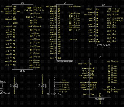
6502ver2.JPG [ 271.04 KiB | Viewed 1410 times ]


applogiz for spelling ..bit I am a bitt dilexic :P


Top
 Profile  
Reply with quote  
PostPosted: Mon Mar 23, 2015 1:11 pm 
Offline
User avatar

Joined: Sun Sep 08, 2013 10:24 am
Posts: 740
Location: A missile silo somewhere under southern England
If you're using EagleCAD to make your design, you can create an 6502.org-approvedTM ( :mrgreen: ) monochrome image by going to:
FILE > EXPOPT > IMAGE
Tick Monochrome
Set the resolution (I usually use 150 (default) or 300)
You can choose to save directly to file (BROWSE to set file location & path) and click OK
Or you can tick Clipboard to copy the image to the windows clipboard for pasting into paint or word, etc..


Top
 Profile  
Reply with quote  
PostPosted: Tue Mar 24, 2015 12:57 am 
Offline

Joined: Mon Jan 07, 2013 2:42 pm
Posts: 576
Location: Just outside Berlin, Germany
chessdoger wrote:
In fact if you use the DS1249 (2Mbit NvRAM) it will give you extra ram as you need. The only issue with nvram is programming it and then making sure the "rom" areas do not get over written as you would have to program them again.


Wait, your idea is to just make everything NVRAM instead of RAM and ROM? Whoa. Hadn't thought of that. Though how would you recover from having, say, your vector locations overwritten?


Top
 Profile  
Reply with quote  
PostPosted: Tue Mar 24, 2015 10:20 am 
Offline
User avatar

Joined: Fri Mar 13, 2015 3:29 am
Posts: 23
scotws wrote:
chessdoger wrote:
In fact if you use the DS1249 (2Mbit NvRAM) it will give you extra ram as you need. The only issue with nvram is programming it and then making sure the "rom" areas do not get over written as you would have to program them again.


Wait, your idea is to just make everything NVRAM instead of RAM and ROM? Whoa. Hadn't thought of that. Though how would you recover from having, say, your vector locations overwritten?


Yep that is the idea .. I trialed nvram with a SC/MP micro Ive been trying to get going .. and it works ..pretty much the same schematic as above (different micro and I used a smaller nvram).

As mentioned if you use the address decoding you can disable the write signal to nvram for areas of ram that are ROM ..ie if you know what area of the code should be permanent ..you can stop the micro from writing into that area by never enabling the write signal ..(once address buss is pointed there)..of course you can read from there :lol:
One other feature to implement ..which I did with the SC/MP is to have a stop or buss disable switch..so when you are ready to power down you halt the buses ..hence stop any changes as you power down.. Of course you cannot stop this is power goes down ..but usually the nvram power protection should kick in and hopefully none of the "ROm" areas of the ram have changed.

In case it has ..have the ram in a ziff socket .. and if need be reprogram nvram and start again :P


Top
 Profile  
Reply with quote  
Display posts from previous:  Sort by  
Post new topic Reply to topic  [ 54 posts ]  Go to page 1, 2, 3, 4  Next

All times are UTC


Who is online

Users browsing this forum: No registered users and 3 guests


You cannot post new topics in this forum
You cannot reply to topics in this forum
You cannot edit your posts in this forum
You cannot delete your posts in this forum
You cannot post attachments in this forum

Search for:
Jump to: