6502.org Forum  Projects  Code  Documents  Tools  Forum
It is currently Sun May 05, 2024 11:19 am

All times are UTC


Post new topic Reply to topic  [ 94 posts ]  Go to page 1, 2, 3, 4, 5 ... 7  Next
Author Message
 Post subject: First steps...
PostPosted: Wed Feb 05, 2014 10:24 pm 
Offline

Joined: Wed Feb 05, 2014 7:02 pm
Posts: 158
Well, after reading the forums a bit, I decided that I will start basic and work my way up to DMA controller... I have a toy application I can think of anyway where I can start with 3 components and add the DMA controller afterward!

First things first, since I tend to forget: Is there a convention for where memory-mapped I/O goes in the 6502? I might be confusing it with another processor, but I seem to recall that I/O goes at the bottom of the address space to avoid conflicting with the vectors.

Secondly, are there any particular limits on the clock speed using perfboard?

I suppose I can ease my limits on using PALs and GALs for logic such as address decoding and basic logic and to save space, but my main problem is I have no way to program them, and would have no clue how to start. Is there any such programmer available that doesn't cost an arm and a leg?

Yes, I need to learn this at some point, but I've never actually successfully soldered a PLCC or surface mount chip (I've tried and failed before, though :D), so for now, it's 40 pin dips :/...

Chances are, I think I will probably use perfboard, IC holders and solder as a prototype. I will have a 65816, PPI, 16550 UART, and an EPROM (yes, I have an EPROM programmer in my PC AT LOL). Eventually, I'd like to add flash ROM and make it so that the whole thing can program it's own memory using a serial ROM routine, but that's a bit later- after I get this working, before the DMA controller.


Then I'll make a part in DipTrace for the 65816 (not too difficult), and then make a PCB that's pluggable into the GPIO slot of a FPGA dev board that I have from university. Since it comes down to it, and the coprocessor-as-DMA idea has been tried and "not worth it", it might be worth the trouble to create a DMA controller in Verilog if there is no equivalent discrete component still manufactured. But this is all later.

Like I've mentioned before, this is a long term project, so any absence on my part doesn't mean I've given up- just real life gets in the way. I will make one more thread tonight regarding my DMA question, but I would appreciate any initial feedback based on what I've said. I've never actually created a system before- just a CPU and memory in Verilog.


Top
 Profile  
Reply with quote  
 Post subject: Re: First steps...
PostPosted: Wed Feb 05, 2014 11:08 pm 
Offline
User avatar

Joined: Thu May 28, 2009 9:46 pm
Posts: 8173
Location: Midwestern USA
cr1901 wrote:
First things first, since I tend to forget: Is there a convention for where memory-mapped I/O goes in the 6502? I might be confusing it with another processor, but I seem to recall that I/O goes at the bottom of the address space to avoid conflicting with the vectors.

Before answering, may I suggest that you read Garth Wilson's 6502 primer? Many of your questions may find answers there.

There is no hard and fast rule on where to place I/O hardware, other than staying out of page one ($0100-$01FF, which is the 6502 hardware stack—which also applies to the 65C816 in emulation mode) and not interfering with the hardware vectors. Some designers map their I/O devices into part of page zero in the assumption that it will improve performance. My opinion is that arrangement is a waste of page zero, which is much more valuable for other purposes. Doing so also complicates decoding logic.

In my POC unit, I map I/O at $D000, with one page assigned to each device. ROM appears at $E000 and extends to $FFFF, for 8KB total. Everything below $D000 is RAM.

Quote:
Secondly, are there any particular limits on the clock speed using perfboard?

Perf board designs have been successfully run at speeds upwards of 8 MHz using wire wrap. However, such an achievement demands relatively meticulous construction, as well as careful layout to keep circuit paths as short as possible. Point-to-point soldered performance will usually not be as good, as short and direct connections are more difficult to achieve.

Quote:
I suppose I can ease my limits on using PALs and GALs for logic such as address decoding and basic logic and to save space, but my main problem is I have no way to program them, and would have no clue how to start. Is there any such programmer available that doesn't cost an arm and a leg?

Relatively inexpensive programmers can be gotten from eBay. If you are going to go this route, I suggest using standard GALs, such as 16V8, 20V10, etc. These devices may also be procured from eBay. I'm partial to Lattice's GALs, which although no longer in production, are still readily available in large quantities. You will also need software to write the logic. WinCUPL, although an Atmel creation, is appropriate and outputs JEDEC-standard fuse maps. Once you make the jump to CPLDs you will need more advanced programming hardware.

That said, I recommend that you start with discrete logic so you gain a full understanding of what your circuit is doing. You can construct a good-performing unit that way and learn the ins and outs of timing analysis and general circuit design. My POC unit is built solely with 74AC discrete logic and will boot at 12.5 MHz.

Quote:
Chances are, I think I will probably use perfboard, IC holders and solder as a prototype. I will have a 65816, PPI, 16550 UART, and an EPROM (yes, I have an EPROM programmer in my PC AT LOL).

Not sure what you are referring to by PPI. As for the 16550, I don't recommend it for a first-time effort. Programming one is not a trivial exercise. Also, there are better UARTs than the 16550, which is mostly an 8250 with thicker paint and shinier pins. :lol: You'd be better off using a 65C51 UART in your first project, which device is relatively easy to program and attaches to the 65C816 buses with a minimum of fuss.

_________________
x86?  We ain't got no x86.  We don't NEED no stinking x86!


Top
 Profile  
Reply with quote  
 Post subject: Re: First steps...
PostPosted: Wed Feb 05, 2014 11:15 pm 
Offline
User avatar

Joined: Fri Aug 30, 2002 1:09 am
Posts: 8432
Location: Southern California
cr1901 wrote:
Well, after reading the forums a bit, I decided that I will start basic and work my way up to DMA controller... I have a toy application I can think of anyway where I can start with 3 components and add the DMA controller afterward!

If you breadboard it (use wire-wrap), you can leave space to add more later. I did that with my workbench computer and built it and got it going in its original form in a week, then kept adding things over the years.

Quote:
First things first, since I tend to forget: Is there a convention for where memory-mapped I/O goes in the 6502? I might be confusing it with another processor, but I seem to recall that I/O goes at the bottom of the address space to avoid conflicting with the vectors.

Part of the 6502 primer: a page on the memory-map requirements.

Quote:
Secondly, are there any particular limits on the clock speed using perfboard?

It depends on too many factors to assign a number. The topic at viewtopic.php?f=4&t=2029&p=17691#p17691 may be helpful. Also, the 6502 primer has a page on construction and avoiding AC-performance problems, at http://wilsonminesco.com/6502primer/construction.html .

Quote:
I suppose I can ease my limits on using PALs and GALs for logic such as address decoding and basic logic and to save space, but my main problem is I have no way to program them, and would have no clue how to start. Is there any such programmer available that doesn't cost an arm and a leg?

Programmable logic would be one more thing to learn; so although it has its benefits, it might be good to leave it for later. Depending on how much RAM and ROM you want, you might be able to do the whole address-decoding scheme with a single 74AC00, as shown approximately at the middle of the page on address decoding, at http://wilsonminesco.com/6502primer/addr_decoding.html in the 6502 primer. This gives 32KB of ROM and 16KB of RAM, and up to ten I/O ICs. (That is a lot of I/O!)

Quote:
Yes, I need to learn this at some point, but I've never actually successfully soldered a PLCC or surface mount chip (I've tried and failed before, though :D), so for now, it's 40 pin dips :/...

You don't have to solder them. There are PLCC sockets, although the wire-wrap ones are very expensive. Wire-wrap is nearly always for making only one of something though, so the cost may be acceptable. These are shown in the middle of the 6502 primer page on getting more on a board, at http://wilsonminesco.com/6502primer/MoreOnPCB.html .

Quote:
Chances are, I think I will probably use perfboard, IC holders and solder as a prototype.

Wire-wrap is much better for this application. See the 6502 primer's page on WW questions and objections answered, at http://wilsonminesco.com/6502primer/WireWrap.html .

Quote:
I will have a 65816, PPI, 16550 UART, and an EPROM (yes, I have an EPROM programmer in my PC AT LOL). Eventually, I'd like to add flash ROM and make it so that the whole thing can program its own memory using a serial ROM routine

EEPROMs can be re-written in-system, but note that you cannot read the EEPROM while it's programming, so your code that keeps checking to see when it's done must be run from RAM (or at least a different EEPROM) before jumping back to any routines in the EEPROM you were programming. Daryl (8BIT here on the forum) tells how to do this, somewhere. You can see the connections in the schematic for a minimal whole computer at the top of the circuit potpourri page of the 6502 primer, at http://wilsonminesco.com/6502primer/pot ... ml#BAS_CPU .

Quote:
Then I'll make a part in DipTrace for the 65816 (not too difficult), and then make a PCB that's pluggable into the GPIO slot of a FPGA dev board that I have from university.

Be sure to read about expansion buses and interfaces on the 6502 primer page by that name, at http://wilsonminesco.com/6502primer/ExpBusIntrfc.html . It is generally not a good idea to run the processor's own buses off the board anymore.

Quote:
Since it comes down to it, and the coprocessor-as-DMA idea has been tried and "not worth it", it might be worth the trouble to create a DMA controller in Verilog if there is no equivalent discrete component still manufactured. But this is all later.

Be sure to check out our topic on transparent DMA, at viewtopic.php?f=1&t=1160. It started out in the context of a 6502, but the 65816 lends itself much better to that since it has the VDA and VPA outputs, and the dead bus cycles can be put to work for DMA without any effect on the processor's performance.

_________________
http://WilsonMinesCo.com/ lots of 6502 resources
The "second front page" is http://wilsonminesco.com/links.html .
What's an additional VIA among friends, anyhow?


Top
 Profile  
Reply with quote  
 Post subject: Re: First steps...
PostPosted: Wed Feb 05, 2014 11:21 pm 
Offline
User avatar

Joined: Thu May 28, 2009 9:46 pm
Posts: 8173
Location: Midwestern USA
GARTHWILSON wrote:
Be sure to check out our topic on transparent DMA, at viewtopic.php?f=1&t=1160. It started out in the context of a 6502, but the 65816 lends itself much better to that since it has the VDA and VPA outputs, and the dead bus cycles can be put to work for DMA without any effect on the processor's performance.

Some of the links are dead, unfortunately.

_________________
x86?  We ain't got no x86.  We don't NEED no stinking x86!


Top
 Profile  
Reply with quote  
 Post subject: Re: First steps...
PostPosted: Sat Feb 08, 2014 4:21 pm 
Offline

Joined: Wed Feb 05, 2014 7:02 pm
Posts: 158
GARTHWILSON wrote:
If you breadboard it (use wire-wrap), you can leave space to add more later. I did that with my workbench computer and built it and got it going in its original form in a week, then kept adding things over the years.
...
Quote:
Chances are, I think I will probably use perfboard, IC holders and solder as a prototype.

Wire-wrap is much better for this application. See the 6502 primer's page on WW questions and objections answered, at http://wilsonminesco.com/6502primer/WireWrap.html.

I probably should have clarified this... once I got a one-off prototype working, the goal will be to design a PCB (will be done in tandem with the prototype)... I imagine a PCB designer can make a more stable, reliable board than I ever could even with wire wrap (Good thinking- I have the tool, need money for posts/spare wire).

If I want to add stuff to the PCB, I can expand the prototype board and get another order. Or I could create stackable modules a la PC104 and actually run the bus off the board- so expansion is trivial. Has the forum invented a bus connector pinout for hobbyists yet? Or perhaps I should wait and just see how the prototype works :P.


GARTHWILSON wrote:
Quote:
Secondly, are there any particular limits on the clock speed using perfboard?

It depends on too many factors to assign a number. The topic at viewtopic.php?f=4&t=2029&p=17691#p17691 may be helpful. Also, the 6502 primer has a page on construction and avoiding AC-performance problems, at http://wilsonminesco.com/6502primer/construction.html .

Although I am a beginner at making my own computer, I consider myself competent in electronics (and willing to fill in the gaps otherwise). To that end, I think from the beginning, I want to design this computer- even in prototype- to support the highest supported clock speed (14MHz). If I keep the first goal small (serial port, PPI, 65816, glue logic, and a RIOT if I can find a 14Mhz version), is this still reasonable goal for the beginner?


GARTHWILSON wrote:
Quote:
Then I'll make a part in DipTrace for the 65816 (not too difficult), and then make a PCB that's pluggable into the GPIO slot of a FPGA dev board that I have from university.

Be sure to read about expansion buses and interfaces on the 6502 primer page by that name, at http://wilsonminesco.com/6502primer/ExpBusIntrfc.html . It is generally not a good idea to run the processor's own buses off the board anymore.

I'm not sure if I have much of a choice here if I want to interface my project to an FPGA board- so that a DMA controller can be developed if necessary. That being said, one of your forum posts mentions that signals should be either next to grounds or virtual grounds to minimize inductance. It's been a while for me- do you have any references offhand that goes over the physics of why this is so (I'm guessing it's transmission-line theory, but I didn't think 14MHz I had to worry about that yet)? I see a number of articles on groundbounce on your site, however, which are also helpful.


GARTHWILSON wrote:
Be sure to check out our topic on transparent DMA, at viewtopic.php?f=1&t=1160. It started out in the context of a 6502, but the 65816 lends itself much better to that since it has the VDA and VPA outputs, and the dead bus cycles can be put to work for DMA without any effect on the processor's performance.

This is actually where my aforementioned question regarding DMA arises. If I understand the timing diagrams of the '816 correctly, VDA and VDP do not go valid until sometime after the leading edge of the clock. That means if VDA and VDP are both not asserted, the DMA controller does not have time to take advantage of the dead bus cycle since the leading edge of the clock has already passed- it will have to wait until the next clock to put the single byte to transfer on the bus, and chances are, the CPU will need the bus again by that time. Or am I missing something?

Additionally, because VDA/VDP do not automatically stop the processor if there is DMA going on, some glue logic is required to assert RDY to stop the CPU* if either VDP/VDA are asserted during the DMA transfer, unless the current instruction has two bus cycles back-to-back where both VDP/VDA are not asserted (only a few, according to the datasheet). As for BE, the signal is asynchronous, so it's as simple as running the output of NAND(VDP, VDA) to BE and the DMA controller's "Request for Bus Granted" input, right?

*From what I understand, RDY will stop the next bus cycle if asserted at the end of the current bus cycle. Since a bus cycle is one clock. This is used for wait states in other processors, but since a bus cycle is one clock on the '816, it can be used to forcefully grab the bus for DMA as well. Contrast with HALT on the z80, which extended the current step in the multiple-long bus cycle. Do I understand this correct? If so, doesn't that mean that DMA can be done without any control signals from the '816.


Top
 Profile  
Reply with quote  
 Post subject: Re: First steps...
PostPosted: Sat Feb 08, 2014 9:15 pm 
Offline
User avatar

Joined: Fri Aug 30, 2002 1:09 am
Posts: 8432
Location: Southern California
cr1901 wrote:
GARTHWILSON wrote:
If you breadboard it (use wire-wrap), you can leave space to add more later. I did that with my workbench computer and built it and got it going in its original form in a week, then kept adding things over the years.
...
Quote:
Chances are, I think I will probably use perfboard, IC holders and solder as a prototype.

Wire-wrap is much better for this application. See the 6502 primer's page on WW questions and objections answered, at http://wilsonminesco.com/6502primer/WireWrap.html.

I probably should have clarified this... once I got a one-off prototype working, the goal will be to design a PCB (will be done in tandem with the prototype)... I imagine a PCB designer can make a more stable, reliable board than I ever could even with wire wrap (Good thinking- I have the tool, need money for posts/spare wire).

Wire-wrap is totally reliable if done right (just follow the recommendations in the primer's Q&A), and can perform pretty well too if done that way, including the prototyping board with at least one plane layer, for a ground plane, and it is used correctly. The Cray-1 running at 80MHz used WW, and some pretty long connections too, although each signal line was paired (twisted) with its ground-return wire. (More on that, below.) A well-done PCB is always better of course; but I've seen hobbyist-designed PCBs that would easily have been outperformed by WW.

Quote:
Has the forum invented a bus connector pinout for hobbyists yet? Or perhaps I should wait and just see how the prototype works :P.

There's no such 6502.org standard.

Quote:
GARTHWILSON wrote:
Quote:
Secondly, are there any particular limits on the clock speed using perfboard?

It depends on too many factors to assign a number. The topic at viewtopic.php?f=4&t=2029&p=17691#p17691 may be helpful. Also, the 6502 primer has a page on construction and avoiding AC-performance problems, at http://wilsonminesco.com/6502primer/construction.html .

Although I am a beginner at making my own computer, I consider myself competent in electronics (and willing to fill in the gaps otherwise). To that end, I think from the beginning, I want to design this computer- even in prototype- to support the highest supported clock speed (14MHz). If I keep the first goal small (serial port, PPI, 65816, glue logic, and a RIOT if I can find a 14Mhz version), is this still reasonable goal for the beginner?

We still don't know what you mean by "PPI." If you keep the board small and follow the guidelines, you can do it. In a well designed circuit, the '816 will usually go well above the rated speed, and in fact the '816 accelerator gizmo that plugged into the back of the Commodore 64 (I can't remember what it's called right now) ran at 20MHz, and you know that they couldn't have run a business on it if there was a significant failure rate from parts not working at that speed. The 6532 RIOT was never made in more than 2MHz AFAIK though, nor was it made in CMOS. You'll want the CMOS parts not just for the lower power consumption and higher speeds, but also for the much greater output drive strength. In my own testing, the WDC 65c22 can pull up to 4.2V with 19mA per pin. NMOS can't pull up that high at all, and even at 2.4V is limited to less than 1mA.

Quote:
GARTHWILSON wrote:
Quote:
Then I'll make a part in DipTrace for the 65816 (not too difficult), and then make a PCB that's pluggable into the GPIO slot of a FPGA dev board that I have from university.

Be sure to read about expansion buses and interfaces on the 6502 primer page by that name, at http://wilsonminesco.com/6502primer/ExpBusIntrfc.html . It is generally not a good idea to run the processor's own buses off the board anymore.

I'm not sure if I have much of a choice here if I want to interface my project to an FPGA board- so that a DMA controller can be developed if necessary. That being said, one of your forum posts mentions that signals should be either next to grounds or virtual grounds to minimize inductance. It's been a while for me- do you have any references offhand that goes over the physics of why this is so (I'm guessing it's transmission-line theory, but I didn't think 14MHz I had to worry about that yet)? I see a number of articles on groundbounce on your site, however, which are also helpful.

The 65 family has so much happening in each cycle that the timings need to be tighter than for its contemporaries that did a bus read or write in say 4 cycles; so we do need to keep our nose clean in that respect. If you have a wire (connector pin, whatever) carrying a signal, and the closest return-path ground conductor is an inch away, you basically have a coil there, with a 1" diameter (irregular shape notwithstanding). That means you have inductance, with all its undesirable effects of radiating the signal, picking up noise from other lines, slowed rise times, resonating with capacitive loads to cause ringing etc.. OTOH, if the return is right next to it like the situation you have with a twisted pair of wires or with a trace against a true ground plane (meaning uninterrupted, unlike the situation you have with a copper pour), then the mutual inductance causes the signal in the signal wire to induce the same current in the opposite direction in the ground return right next to it, cancelling out the unwanted effects we had in the first situation. The return current does not take the shortest path, but follows as closely as possible the path of the signal line. Even in a PC board with a ground plane, the return current goes immediately under the trace, taking the shape of the trace, since that's what's easiest, because of mutual inductance.

Quote:
GARTHWILSON wrote:
Be sure to check out our topic on transparent DMA, at viewtopic.php?f=1&t=1160. It started out in the context of a 6502, but the 65816 lends itself much better to that since it has the VDA and VPA outputs, and the dead bus cycles can be put to work for DMA without any effect on the processor's performance.

This is actually where my aforementioned question regarding DMA arises. If I understand the timing diagrams of the '816 correctly, VDA and VDP do not go valid until sometime after the leading edge of the clock. That means if VDA and VDP are both not asserted, the DMA controller does not have time to take advantage of the dead bus cycle since the leading edge of the clock has already passed- it will have to wait until the next clock to put the single byte to transfer on the bus, and chances are, the CPU will need the bus again by that time. Or am I missing something?

VDA and VPA are guaranteed to be valid sooner than the bank address is guaranteed to be, with the same timing spec as the lower 16 address bits. This is before phase 2 rises, so there's definitely time.

Quote:
Additionally, because VDA/VDP do not automatically stop the processor if there is DMA going on, some glue logic is required to assert RDY to stop the CPU* if either VDP/VDA are asserted during the DMA transfer, unless the current instruction has two bus cycles back-to-back where both VDP/VDA are not asserted (only a few, according to the datasheet).

The point of the transparent DMA is that you don't stop the processor at all, even for a single cycle. You only step in when it's not using the bus. There is no need to have two dead bus cycles back to back; but if you're writing to the same addresses at the same time that the processor is (which is probably asking for trouble in this context), you can use ML\ to make sure you don't cut in on a RMW instruction.

hopefully someone else can answer the other questions better than I think I could.

_________________
http://WilsonMinesCo.com/ lots of 6502 resources
The "second front page" is http://wilsonminesco.com/links.html .
What's an additional VIA among friends, anyhow?


Top
 Profile  
Reply with quote  
 Post subject: Re: First steps...
PostPosted: Sat Feb 08, 2014 9:23 pm 
Offline

Joined: Wed Feb 05, 2014 7:02 pm
Posts: 158
What I meant was... a DMA controller is a sequential circuit, correct- it will only latch vda/vdp of the current bus cycle during the next leading edge of the next phase 2 clock... And vda/vdp serves as the DMA acknowledge signal in the context of cycle steal DMA, right?

PPI is another name for the 8255 from intel.


Top
 Profile  
Reply with quote  
 Post subject: Re: First steps...
PostPosted: Sat Feb 08, 2014 9:50 pm 
Offline
User avatar

Joined: Fri Aug 30, 2002 1:09 am
Posts: 8432
Location: Southern California
.
I made a few edits to my post above as you were writing.

Quote:
What I meant was... a DMA controller is a sequential circuit, correct- it will only latch vda/vdp of the current bus cycle during the next leading edge of the next phase 2 clock... And vda/vdp serves as the DMA acknowledge signal in the context of cycle steal DMA, right?

The 6502 & '816 use a lot of transparent latches in the design, rather than edge-triggered registers. Even the separate address bank latch IC is transparent while phase 2 is low, so the things out on the bus can get started handling the address before phase 2 rises. The 65c22 and other 65-family I/O ICs require the chip-select and register-select and R/W\ lines to be valid and stable a certain amount of time before phase 2 rises. It may be a different concept to get used to, compared to other processors.

BTW:
VDA = valid data address
VPA = valid program address
VPB = vector pull not
There's no "VDP" pin.

_________________
http://WilsonMinesCo.com/ lots of 6502 resources
The "second front page" is http://wilsonminesco.com/links.html .
What's an additional VIA among friends, anyhow?


Top
 Profile  
Reply with quote  
 Post subject: Re: First steps...
PostPosted: Sat Feb 08, 2014 10:13 pm 
Offline

Joined: Wed Feb 05, 2014 7:02 pm
Posts: 158
So this basically means that standalone DMA ICs such as the 8237 will not work with the 65xx family because they are edge triggered? I need an IC that can asynchronously respond to (or as you say, transparently latch) VDA and VPA being pulled low, and which can still prepare all the control signals to transfer a byte before the rising edge of Phi2?

As an example, Ignoring the fact that the 8237 cannot transfer a byte in one full clock cycle (it requires at least 2), it will not even start a DMA transfer until the leading edge of the next clock cycle after it receives a "DMA Acknowledge"- in other words, the leading edge after when VDA and VPA are both low (sorry, I was typing on a tablet and had Sega Genesis on the mind when I wrote VDP XD).


Top
 Profile  
Reply with quote  
 Post subject: Re: First steps...
PostPosted: Fri Mar 07, 2014 5:33 am 
Offline

Joined: Wed Feb 05, 2014 7:02 pm
Posts: 158
GARTHWILSON wrote:
hopefully someone else can answer the other questions better than I think I could.


Apologies for not responding to this when you initially posted this. I did a poor job in retrospect trying to explain why I'm having issues. I will come back to my DMA question when I reach that point, as it's the final portion of "round 1" of this project.

Okay, so I've reached a suitable stopping point for my current VCF activity, so time for me to make some more progress on this front :D!

In order to interface to a development board, I need to be able to route the 816 bus off the board unfortunately. If I design a preliminary bus "standard", would someone be willing to critique it for me? My dev board uses a 40-pin male IDE connector for GPIO, so I'd need to use a female IDE connector that solders underneath the PCB. I know this is explicitly not recommended in the primer- I'm willing to take the risks to life, property, and my assets in this case.

I'm actually doing the paper design now... I'll start out simple, as suggested in previous posts... '816, RAM, ROM, VIA, 6551, and two banks (mix of code/data, or one code and one data- haven't decided yet). Since this is effectively will become an exercise in creating a DMA controller, however, I want to get started on that as early as practically possible. Might be an odd goal for a project, but since this is a "toy CPU system design" anyway, I have no qualms about it :P. And besides, might as well USE the not widely used features of the '816 :).


Top
 Profile  
Reply with quote  
 Post subject: Re: First steps...
PostPosted: Fri Mar 07, 2014 6:48 pm 
Offline
User avatar

Joined: Thu May 28, 2009 9:46 pm
Posts: 8173
Location: Midwestern USA
cr1901 wrote:
In order to interface to a development board, I need to be able to route the 816 bus off the board unfortunately.

In which case, I suggest you look at using drivers for the address bus (74AC541, for example, two required) and a transceiver (74AC245) for the data bus. The drivers and transceiver will help to mitigate the effects of bus loading. Note that everything should be on the "downstream" side of the drivers and transceiver to avoid inadvertent signal skew. Bus termination will likely be necessary to control ringing, an area where you may have to experiment to achieve satisfactory results. Thevenin termination may suffice if the aggregate bus length isn't too great.

You will also need a latch for capturing the bank address (74ABT573 or 74AC573, the former is the faster part) and a two-phase clock generator to control the latch and transceiver output-enables. See attached clock generator schematic, as well as bus logic example—ABx and DBx connections on the drivers, latch and transceiver are connected to the MPU's address and data bus pins, respectively.

Note that use of the clock to determine when the transceiver should be active doesn't automatically meet the requirement of not reading or writing during Ø2 low. That is accomplished by qualifying RWB with Ø2. Such qualification is not necessary with the W65C21x, W65C22x and W65C51x, and should not be applied—connect RWB of these devices directly to RWB on the 65C816.

Also note that VDA and VPA must be consulted in determining when to latch the bank address. A number of instructions cause the '816 to generate false address bus states during intermediate execution steps, especially when indexing is involved to determine the effective address. If the expression VDA | VPA is false (| meaning logical OR) then the address bus content is undefined and chip enables must not be asserted. However, during that time, your DMA controller could temporarily become the bus master by negating BE—the '816 will continue with what it is doing. If one or two "dead" cycles don't give the controller enough time to accomplish anything, then it will have to "forceably" kick the MPU off the buses by negating RDY and BE (in that order), do its work and then restart the MPU by releasing BE and RDY (in that order). The MLB signal would have to be factored into any bus mastering as well.

Quote:
If I design a preliminary bus "standard", would someone be willing to critique it for me? My dev board uses a 40-pin male IDE connector for GPIO, so I'd need to use a female IDE connector that solders underneath the PCB. I know this is explicitly not recommended in the primer- I'm willing to take the risks to life, property, and my assets in this case.

As long as you understand the perils and promise not to sue us, we'll try to help out. :lol:

Jocosity aside, a viable expansion bus design, that is, one into which cards could be plugged, is better developed so that it is isolated from the MPU bus, a la PCI in modern x86 machines. This could be accomplished with the W65C21 or W65C22, or similar devices. Use of peripheral silicon to drive the expansion bus instead of attaching it to the MPU's buses means that the expansion bus becomes a memory-mapped "I/O device," and thus can't affect the MPU unless the latter allows it to. It also means that the expansion bus speed can be independent of the Ø2 clock rate. There is a bit more to this than just wiring some address and data lines to some connectors.

Quote:
I'm actually doing the paper design now... I'll start out simple, as suggested in previous posts... '816, RAM, ROM, VIA, 6551, and two banks (mix of code/data, or one code and one data- haven't decided yet).

It would probably be wise to not segregate code and data. If you are thinking about implementing a Harvard architecture, you can only do part of it. A true Harvard machine has the code and data storage physically separated and connected to the MPU by different buses. You wouldn't be able to have separate buses with the '816. Just an opinion, but I see no upside to trying to go the Harvard route in a hobby machine.

You always have the option to load your program wherever you choose, as long as it is no longer than 64K. Data can exceed 64K, as indexing past the end of one bank always temporarily increments to the next bank (but doesn't actually change DB). You can also use indirect indexed long addressing (e.g., LDA [$80],Y) to reach out to any bank and span into the next one.

Quote:
And besides, might as well USE the not widely used features of the '816 :).

I've been an advocate of that all along. :lol: You'll get ample opportunity when you reach the stage of trying to implement DMA.

Attachment:
File comment: Two-Phase Clock Generator
clock_gen_2p.gif
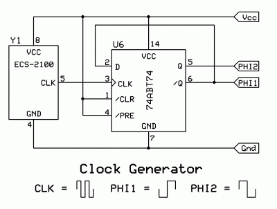
clock_gen_2p.gif [ 53.85 KiB | Viewed 1868 times ]

Attachment:
File comment: 65C816 Bus Drivers & Bank Latch Example
816_bus_logic.gif
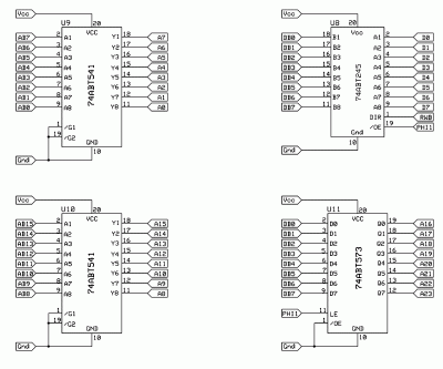
816_bus_logic.gif [ 84.25 KiB | Viewed 1868 times ]

_________________
x86?  We ain't got no x86.  We don't NEED no stinking x86!


Top
 Profile  
Reply with quote  
 Post subject: Re: First steps...
PostPosted: Sat Mar 08, 2014 12:46 am 
Offline

Joined: Wed Feb 05, 2014 7:02 pm
Posts: 158
Got a '816 part made in DipTrace :D... moving on to the VIA...

I made a DIP and PLCC part, but before I continue:

As I've mentioned before, I want to START at a high clock speed, not work my way up to it (I'll do wire wrap but I'll make the PCB in tandem). Is it possible to run a wire-wrapped DIP40 '816 at 14MHz reliably? This thread seems to say that PLCC is essentially required at that speed.

Also, I seem to recall that there is a method to run the 816 bus off the PCB without sacrificing half the connections for ground wires... can anyone elaborate on how that might be done while preserving signal integrity?


Top
 Profile  
Reply with quote  
 Post subject: Re: First steps...
PostPosted: Sat Mar 08, 2014 1:21 am 
Offline
User avatar

Joined: Fri Aug 30, 2002 1:09 am
Posts: 8432
Location: Southern California
cr1901 wrote:
As I've mentioned before, I want to START at a high clock speed, not work my way up to it (I'll do wire wrap but I'll make the PCB in tandem). Is it possible to run a wire-wrapped DIP40 '816 at 14MHz reliably? This thread seems to say that PLCC is essentially required at that speed.

Perhaps you'll be our guinnea pig? :lol: I hope the WW'ed DIP would work, but I'm not confident enough to take my own time to build it and risk the possibility that it won't work.

Quote:
Also, I seem to recall that there is a method to run the 816 bus off the PCB without sacrificing half the connections for ground wires... can anyone elaborate on how that might be done while preserving signal integrity?

If you use an actual ribbon, then every other conductor being ground is best (like they do for disc drives), especially because of the length. Power, bypassed to ground at the connectors, serves the purpose too. But for boards being plugged into each other, you can get reasonably close to the goal by distributing the grounds and bypassed power lines such that the closest return for any given signal line is not far away, say just over .2" like I have on my 10ns 5V 4Mx8 SRAM module. You can see the pinout on page 2 of http://wilsonminesco.com/WM-1_4Mx8SRAMm ... -15-13.pdf .

_________________
http://WilsonMinesCo.com/ lots of 6502 resources
The "second front page" is http://wilsonminesco.com/links.html .
What's an additional VIA among friends, anyhow?


Top
 Profile  
Reply with quote  
 Post subject: Re: First steps...
PostPosted: Sat Mar 08, 2014 2:12 am 
Offline

Joined: Wed Feb 05, 2014 7:02 pm
Posts: 158
GARTHWILSON wrote:
Perhaps you'll be our guinnea pig? :lol: I hope the WW'ed DIP would work, but I'm not confident enough to take my own time to build it and risk the possibility that it won't work.

Might as well... if it doesn't work, it doesn't work- I just lower the clock speed until it does... and take it into consideration during "round 2".

GARTHWILSON wrote:
If you use an actual ribbon, then every other conductor being ground is best (like they do for disc drives), especially because of the length. Power, bypassed to ground at the connectors, serves the purpose too. But for boards being plugged into each other, you can get reasonably close to the goal by distributing the grounds and bypassed power lines such that the closest return for any given signal line is not far away, say just over .2" like I have on my 10ns 5V 4Mx8 SRAM module. You can see the pinout on page 2 of http://wilsonminesco.com/WM-1_4Mx8SRAMm ... -15-13.pdf .


What if the ribbon cable is of short length, i.e. only 3 inches or so? This would be most ideal if only because finding a female IDE connector to attach directly to the bottom of the board might be difficult (the dev board's GPIO is exposed through a male IDE connector). Otherwise, I'll need to use 80 conductors XD (each ribbon connector on the dev board has room for 40 GPIO... some of the signals obviously aren't needed, but 20 signal pins isn't enough- a minimum of 25, 24 ADDR/DATA, and PHI2 are needed).


Top
 Profile  
Reply with quote  
 Post subject: Re: First steps...
PostPosted: Sat Mar 08, 2014 2:34 am 
Offline

Joined: Wed Feb 05, 2014 7:02 pm
Posts: 158
One other thing I forgot... I was looking up whether I'd need bus drivers or not, and Garth's post in this thread states that typically, you do not need them for the CMOS parts:

GARTHWILSON wrote:
Between bus capacitance and the output-buffer and timing specifications of WDC's 65c02 being quite conservative, actual use becomes much easier than one might expect. What you are proposing and asking is rather common for newcomers to the 6502, but far more complex than necessary. The bus buffer for example will only slow things down, and it's not needed even for DMA since WDC's 65c02 has a BE (bus-enable) input pin (pin 36 on the DIP), ML (memory lock) output pin (pin 5 on the DIP), and VP (vector pull) output pin (pin 1 on the DIP) so you can tri-state the processor's buses at appropriate times for DMA.

DMA aside, if you can get away with 32KB of ROM and 16KB of RAM (or vice-versa with a small change) and up to 10 I/O ICs, the diagram at http://www.6502.org/users/garth/project ... chematic=2 will do the job using only a single 74xx00 for address decoding, and even leave one section available for something else. Gate delays are minimal, so you can achieve high clock rates. I need to update my pages on my workbench computer to reflect recent expansion, but I am still using this glue logic scheme. With 4MHz parts, the first problems show up at just over 7MHz at room temperature, so I run it at 5MHz for some margin. I have hundreds of systems flying in aircraft with the same scheme, and none has ever had a problem.


For an initial system, even with DMA, I can see the logic. However, what happens when the drive strength of the '816 is no longer sufficient when you start adding more peripherals? Will the new delay from the bus drivers cause the initial design at the original clock speed to go kaput? And would a hypothetical DMA controller need to disable the bus driver as well, or would the BE pin be sufficient?

I can't think of any conflicts offhand, but just for "preventative maintenance :P", would the addition of a bus driver on the address/data lines cause any conflicts with the process of cycle-steal DMA?

I should probably look at the original IBM PC schematic for an example...


Top
 Profile  
Reply with quote  
Display posts from previous:  Sort by  
Post new topic Reply to topic  [ 94 posts ]  Go to page 1, 2, 3, 4, 5 ... 7  Next

All times are UTC


Who is online

Users browsing this forum: No registered users and 5 guests


You cannot post new topics in this forum
You cannot reply to topics in this forum
You cannot edit your posts in this forum
You cannot delete your posts in this forum
You cannot post attachments in this forum

Search for:
Jump to: