6502.org Forum  Projects  Code  Documents  Tools  Forum
It is currently Thu May 23, 2024 3:57 am

All times are UTC


Post new topic Reply to topic  [ 8 posts ] 
Author Message
PostPosted: Wed Apr 15, 2020 5:12 pm 
Offline

Joined: Fri Nov 16, 2018 8:55 pm
Posts: 71
I "get" that memory mapping allows RAM/registers from one device to be overlayed into system RAM on a main device. I'm sure there is a more formal definition that I've run a fowl of with that statement. Nonetheless, it's the mechanism that lets me poke into system RAM on a C64 and have it "do stuff" with the VIC-II chip, the SID chip, etc.

What I don't get is how it gets implemented in the first place. I've always just taken for granted that it "just works."

So, let me ask: given an arbitrary chip/widget and a 6502 and 64k of RAM how do you create a memory mapping between the two in the first place?


Top
 Profile  
Reply with quote  
PostPosted: Wed Apr 15, 2020 5:29 pm 
Offline

Joined: Thu Mar 12, 2020 10:04 pm
Posts: 690
Location: North Tejas
Circuitry is used to respond to specific combinations of the address lines to "enable" memory chips at their appropriate addresses.

Similar circuitry is used to decode the addresses of I/O devices.


Top
 Profile  
Reply with quote  
PostPosted: Wed Apr 15, 2020 5:44 pm 
Offline
User avatar

Joined: Thu Dec 11, 2008 1:28 pm
Posts: 10802
Location: England
The particular thing mentioned is, I think, where reads are directed to one device and writes to another: which 'just' means using the RnW signal somewhat like another address signal, in the address decoding.

It's the address decoding which determines which device responds to the CPU's accesses: generally by controlling Chip Enable inputs to all devices: just one device gets an active Chip Enable, and so just one device responds to the access.

It would be relatively common, for example, to direct reads to ROM and writes to screen memory, which allows the two areas to overlap in the same address range.

If peripherals are read/write, that in itself isn't quite enough.

But in some machines, 64k RAM doesn't mean the whole 64k: almost all of the RAM is accessible, but some addresses are still decoded to peripheral devices.

In the C64, AIUI, addresses 0000 and 0001 are always directed to registers controlling the CPU's own control outputs, which are used in the address decoding.


Top
 Profile  
Reply with quote  
PostPosted: Wed Apr 15, 2020 5:48 pm 
Offline
User avatar

Joined: Fri Dec 12, 2008 10:40 pm
Posts: 1002
Location: Canada
Your system's memory map is simply how the memory space is utilized.

With the 6502 in particular (and some other CPUs) the I/O device registers (how you communicated with those devices) must also be in that memory space. So, in it's most common form, the hardware memory map of a 6502 would contain RAM, I/O and ROM. The 6502 utilizes page 0 of it's memory space (the lowest 256 bytes) for a particular kind of addressing which reduces the clock cycles of instruction executed on that page. It also requires that interrupt and reset vectors exist in the last 6 bytes of the memory space. Typically then, the 6502 would have RAM mapped in the lower addresses, ROM mapped in the higher address and the I/O mapped somewhere in between.

And then there is also software memory mapping ... that deals with what routines, data and vectors go where in the memory space.

_________________
Bill


Top
 Profile  
Reply with quote  
PostPosted: Wed Apr 15, 2020 5:52 pm 
Offline
User avatar

Joined: Thu Dec 11, 2008 1:28 pm
Posts: 10802
Location: England
BTW see also
https://www.c64-wiki.com/wiki/Bank_Switching
and pages linked from there. Edit: especially
https://www.c64-wiki.com/wiki/Zeropage
which describes the control bits LORAM HIRAM CHAREN


Top
 Profile  
Reply with quote  
PostPosted: Wed Apr 15, 2020 7:10 pm 
Offline
User avatar

Joined: Wed Feb 14, 2018 2:33 pm
Posts: 1417
Location: Scotland
load81 wrote:
I "get" that memory mapping allows RAM/registers from one device to be overlayed into system RAM on a main device. I'm sure there is a more formal definition that I've run a fowl of with that statement. Nonetheless, it's the mechanism that lets me poke into system RAM on a C64 and have it "do stuff" with the VIC-II chip, the SID chip, etc.

What I don't get is how it gets implemented in the first place. I've always just taken for granted that it "just works."

So, let me ask: given an arbitrary chip/widget and a 6502 and 64k of RAM how do you create a memory mapping between the two in the first place?


Slightly simplified, but:

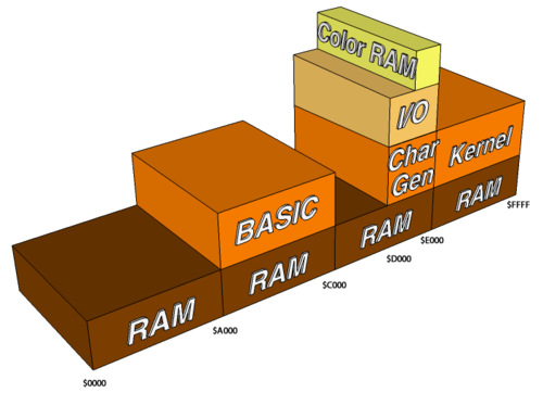
The CPU address bus is connected to all peripherals. (e.g. RAM, ROM, Sound Chip, Graphics controller, etc.)

Peripherals have an "enable" signal input. They see the changing address bus (and data bus) but stay dormant until their enable signal input is set.

Other devices/chips connect to the CPU address bus and decode the addresses and create the enable signals that connect to the peripherals.

Some peripherals also use the bottom address line or 3 - e.g. the 6522 VIA has 16 registers, so as well as it's enable input, it further decodes internally using the bottom 4 address lines

The decoder device(s) would be a comparator (match 8 inputs from 8 address lines to a fixed value), or a set of TTL logic gates or some other complex logic like a GAL or CPLD. A simple example might be:

Code:
Address is $0000 through $7FFF -> Set RAM enable signal
Address is $8000 through $FDFF -> Set ROM enable signal
Address is $FE00 through $FEFF -> Set VIA enable signal
Address is $FF00 through $FFFF -> Set ROM enable signal


That would create a "hole" in the ROM for some peripherals.

and that's essentially that. The decoding can be as simple (as above) or as complex (e.g. 4 x VIAs, 2 UARTs, RAM, ROM, Video chips, sound chips, joystick, and so on) as you want on your board.

-Gordon

_________________
--
Gordon Henderson.
See my Ruby 6502 and 65816 SBC projects here: https://projects.drogon.net/ruby/


Top
 Profile  
Reply with quote  
PostPosted: Wed Apr 15, 2020 7:12 pm 
Offline
User avatar

Joined: Thu Dec 11, 2008 1:28 pm
Posts: 10802
Location: England
As ever, Garth's primer could help here - there's a section on address decoding.
http://wilsonminesco.com/6502primer/


Top
 Profile  
Reply with quote  
PostPosted: Wed Apr 15, 2020 7:17 pm 
Offline
User avatar

Joined: Thu Dec 11, 2008 1:28 pm
Posts: 10802
Location: England
Also note that the C64 is special: it's not a basic 6502 such as a person would design for themselves. There's an excellent picture on this page:
Ram under Rom - a brief look into C64 memory


Image


Top
 Profile  
Reply with quote  
Display posts from previous:  Sort by  
Post new topic Reply to topic  [ 8 posts ] 

All times are UTC


Who is online

Users browsing this forum: No registered users and 1 guest


You cannot post new topics in this forum
You cannot reply to topics in this forum
You cannot edit your posts in this forum
You cannot delete your posts in this forum
You cannot post attachments in this forum

Search for:
Jump to: