6502.org Forum  Projects  Code  Documents  Tools  Forum
It is currently Sat Apr 27, 2024 9:13 pm

All times are UTC


Post new topic Reply to topic  [ 8 posts ] 
Author Message
 Post subject: Cupl .LQ extension
PostPosted: Mon Jun 26, 2023 10:12 pm 
Offline
User avatar

Joined: Sat Jul 24, 2021 1:37 pm
Posts: 282
Hello! I've been trying to use the .LQ extension in WinCUPL to define an input latch for my '816 bank address. According to Atmel's WinCUPL User's Manual:

Attachment:
Screenshot 2023-06-26 at 23.56.53.png
Screenshot 2023-06-26 at 23.56.53.png [ 95.56 KiB | Viewed 4073 times ]


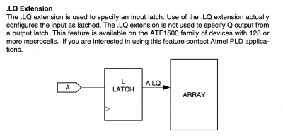
According to the Devhelp.pdf file in WinCUPL's installation, my ATF1508 indeed supports this extension:

Attachment:
Screenshot 2023-06-26 at 23.56.10.png
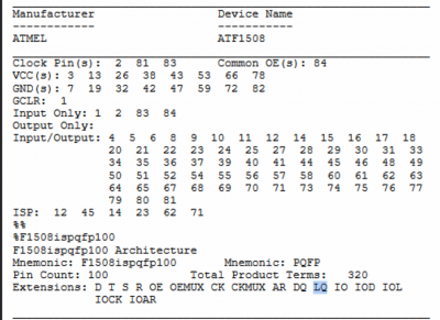
Screenshot 2023-06-26 at 23.56.10.png [ 290.72 KiB | Viewed 4073 times ]


However, I haven't found any examples showing how to configure this latch, specifically its clock. I've tried the following (also with .IOCK and .CKMUX for good measure), which results in the fitter not producing any output / crashing.

Code:
PIN 1     = CLK ;
PIN     = [DBA0..7];
PIN     = [A16..23];

[A16..23] = [DBA0..7].LQ;
[DBA0..7].CK = CLK;


Here is the output from the fitter

Code:
Atmel ATF1508AS Fitter Version 1.8.7.8 ,running Tue Jun 27 00:03:46 2023


fit1508 C:\WINCUPL\WINCUPL\BB816.tt2 -CUPL -dev P1508C84 -JTAG ON


****** Initial fitting strategy and property ******
 Pla_in_file = BB816.tt2
 Pla_out_file = BB816.tt3
 Jedec_file = BB816.jed
 Vector_file = BB816.tmv
 verilog_file = BB816.vt
 Time_file =
 Log_file = BB816.fit
 err_file =
 Device_name = PLCC84
 Module_name =
 Package_type = PLCC
 Preassign_file =
 Property_file =
 Sleep_mode =
 Preassignment =
 Security_mode = OFF
 Pin_keep_mode = ON
 Dedicated_input_clock =
 Dedicated_input_reset =
 Dedicated_input_oe =
 supporter = CUPL
 optimize = ON
 Soft_buffer =
 Xor_synthesis = OFF
 Foldback_logic =  on
 Expander =
 Cascade_logic = OFF
 Dedicated_input =
 Output_fast = OFF
 *******************************
 Power down pin 1 = OFF
 Power down pin 2 = OFF
 power_reset = OFF
 JTAG = ON
 TDI pullup = ON
 TMS pullup = ON
 MC_power = OFF
 Open_collector = OFF
 ITD0 = ON
 ITD1 = ON
 ITD2 = ON
 Fast_inlatch = off
 *******************************


Replacing the two lines with only "[A16..23] = [DBA0..7];" gives me an output in the fitter, so I'm pretty sure this extension is the problem.
Has anyone looked into this before? I'm worried about the "Contact Atmel PLD applications" prompt, if it means you need some special incantation to use the functionality.

_________________
BB816 Computer YouTube series


Top
 Profile  
Reply with quote  
 Post subject: Re: Cupl .LQ extension
PostPosted: Mon Jun 26, 2023 10:33 pm 
Offline
User avatar

Joined: Sat Jul 24, 2021 1:37 pm
Posts: 282
Looking at the macrocell, this definitely seems to be an option, which points to a cupl syntax problem. From this diagram, my inclination would be to use .CK to define the clock for that latch, but I must be missing something.

Attachment:
Screenshot 2023-06-27 at 00.30.44.png
Screenshot 2023-06-27 at 00.30.44.png [ 219.07 KiB | Viewed 4065 times ]

_________________
BB816 Computer YouTube series


Top
 Profile  
Reply with quote  
 Post subject: Re: Cupl .LQ extension
PostPosted: Mon Jun 26, 2023 11:19 pm 
Offline

Joined: Fri Jul 09, 2021 10:12 pm
Posts: 741
Just a guess, but since latches have a latch enable input rather than a clock input, does it want ".LE" (like it would for an output latch) rather than any type of ".CK"?


Top
 Profile  
Reply with quote  
 Post subject: Re: Cupl .LQ extension
PostPosted: Tue Jun 27, 2023 12:15 am 
Offline
User avatar

Joined: Thu May 28, 2009 9:46 pm
Posts: 8144
Location: Midwestern USA
Try .LE (latch enable).

_________________
x86?  We ain't got no x86.  We don't NEED no stinking x86!


Top
 Profile  
Reply with quote  
 Post subject: Re: Cupl .LQ extension
PostPosted: Tue Jun 27, 2023 6:28 am 
Offline
User avatar

Joined: Sat Jul 24, 2021 1:37 pm
Posts: 282
Doesn't do the trick:

Quote:
[A16..23] = [DBA0..7].LQ;
[DBA0..7].LE = CLK;


Results in a blank output from the fitter

_________________
BB816 Computer YouTube series


Top
 Profile  
Reply with quote  
 Post subject: Re: Cupl .LQ extension
PostPosted: Tue Jun 27, 2023 6:46 am 
Offline

Joined: Sun Jun 29, 2014 5:42 am
Posts: 337
akohlbecker wrote:
However, I haven't found any examples showing how to configure this latch, specifically its clock. I've tried the following (also with .IOCK and .CKMUX for good measure), which results in the fitter not producing any output / crashing.

In cases where the fitter crashes, you can often see a more helpful error message if you run it manually from a command prompt.

Can you post your complete example?

Dave


Top
 Profile  
Reply with quote  
 Post subject: Re: Cupl .LQ extension
PostPosted: Tue Jun 27, 2023 12:49 pm 
Offline
User avatar

Joined: Sat Jul 24, 2021 1:37 pm
Posts: 282
Alright, I've experimented a bunch, and I think I found a solution to my problem. I did not manage to make use of the .LQ extension, but I was able to implement it like this. The code below implements a simplified bank address latch and data bus buffer for a 65C816 (including BANK0 as an example of using the latched outputs). I'm still waiting on my adapter boards so I haven't tested it on device.

Code:
Name     test816 ;
PartNo   00 ;
Date     26/06/2023 ;
Revision 01 ;
Designer Adrien Kohlbecker ;
Company  - ;
Assembly None ;
Location  ;
Device   f1508ispplcc84 ;

/* Enable pull ups on JTAG interface */
PROPERTY ATMEL { TDI_PULLUP = ON };
PROPERTY ATMEL { TMS_PULLUP = ON };

PIN 1 = CLK;
PIN   = [DBA0..7];
PIN   = [A16..23];
PIN   = [D0..7];
PIN   = RWB;
PIN   = ! BANK0;

[D0..7] = [DBA0..7].IO;
[D0..7].OE = CLK & !RWB;

[DBA0..7] = [D0..7].IO;
[DBA0..7].OE = CLK & RWB;

[A16..23].L = [DBA0..7].IO;
[A16..23].LE = CLK;

BANK0 = !(A16 # A17 # A18 # A19 # A20 # A21 # A22 # A23);


By connecting A16.L to DBA0.IO, and setting A16.LE to CLK, it implements the correct latching. Now, it uses the latch located at the A16 pin, not the one at the DBA0 pin, but I'm not sure if that makes a difference? :?: I'm wondering if this could impact the propagation delay on downstream signals such as BANK0 when the latch is open. If BANK0's combinatorial inputs come through DBA0's input then internally through the latch at A16, rather than directly through the latch at DBA0. Is there an additional delay due to the path between DBA0 and A16?

Attached is the output of the fitter.


Attachments:
test816.txt [22.8 KiB]
Downloaded 52 times

_________________
BB816 Computer YouTube series


Last edited by akohlbecker on Tue Jun 27, 2023 1:11 pm, edited 1 time in total.
Top
 Profile  
Reply with quote  
 Post subject: Re: Cupl .LQ extension
PostPosted: Tue Jun 27, 2023 1:05 pm 
Offline
User avatar

Joined: Sat Jul 24, 2021 1:37 pm
Posts: 282
In case this helps to figure it out, here are some of the steps I took. Thanks Dave for suggesting the command line, as the errors are indeed better reported.

Code:
A16 = DBA0.LQ;


Gives me a fitter error:

Code:
Error - Node DBA0 is latched and there is no .LE or .LH in .olb


If I add to this

Code:
DBA0.LE = CLK;


I get the same message, and also cupl.exe reports

Code:
[0014cc] Please note: unknown extension encountered:


If I then try to setup the input latch manually with

Code:
DBA0.L = DBA0.IO;


I get the same cupl extension error, and the fitter reports

Code:
Error on line 27 : Incorrect variable list (variable duplication)


With this PLA input file (line 27 is .phase)

Code:
#$ TOOL CUPL
# Berkeley PLA format generated using CUPL(WM) 5.0a
# Serial#  MW-10400000
# Created  Tue Jun 27 15:09:06 2023
#
#    Name        test816
#    Partno      00
#    Revision    01
#    Date        26/06/2023
#    Designer    Adrien Kohlbecker
#    Company     -
#    Assembly    None
#    Location   
#
#$ TITLE  test816
#$ PROPERTY ATMEL TDI_PULLUP = ON
#$ PROPERTY ATMEL TMS_PULLUP = ON
#$ MODULE  test816
#$ JEDECFILE  test816
#$ DEVICE  f1508ispplcc84
#$ PINS  27 A16+ A17+ A18+ A19+ A20+ A21+ A22+ A23+ BANK0+ CLK+:1 D0+ D1+ D2+ D3+ D4+ D5+ D6+ D7+ DBA0+ DBA1+ DBA2+ DBA3+ DBA4+ DBA5+ DBA6+ DBA7+ RWB+
.i 5
.o 6
.type f
.ilb  CLK D0.PIN DBA0.PIN DBA0.L RWB
.ob   A16 D0 D0.OE DBA0 DBA0 DBA0
.phase 111111
.p 5
---1- 100000
--1-- 010010
1---0 001000
-1--- 000100
1---- 000001
.e


I'm not sure what that means.

_________________
BB816 Computer YouTube series


Top
 Profile  
Reply with quote  
Display posts from previous:  Sort by  
Post new topic Reply to topic  [ 8 posts ] 

All times are UTC


Who is online

Users browsing this forum: No registered users and 11 guests


You cannot post new topics in this forum
You cannot reply to topics in this forum
You cannot edit your posts in this forum
You cannot delete your posts in this forum
You cannot post attachments in this forum

Search for:
Jump to: