6502.org Forum  Projects  Code  Documents  Tools  Forum
It is currently Mon May 06, 2024 8:35 am

All times are UTC


Post new topic Reply to topic  [ 81 posts ]  Go to page Previous  1, 2, 3, 4, 5, 6  Next
Author Message
 Post subject: Re: CPLD + 6502 Trainer
PostPosted: Fri Feb 04, 2022 7:00 pm 
Offline

Joined: Fri Dec 21, 2018 1:05 am
Posts: 1076
Location: Albuquerque NM USA
This is a RAM diagnostic that first checks the zero page and stack ($0-$1FF) without using any RAM resources. Once ZP and stack tests passed, it uses ZP and stack to run full RAM test from $200-$DFFF. RAM test is attached. The hardware has successfully passed RAM diagnostic at 7.37MHz.
Attachment:
CPLD Trainer memory diagnostic.jpg
CPLD Trainer memory diagnostic.jpg [ 62.74 KiB | Viewed 7717 times ]


Since all active components are populated, I'm trying higher frequency system clock to find out the design margin. The RAM test will run OK with 11MHz oscillator, but won't sign on with 14.7MHz oscillator, even with faster EPROM (W27C512-45Z 45nS). Adding one wait state to EPROM access allows it to run test up to 18.4MHz. At 22MHz EPROM is able to boot and test RAM but zero page and stack test failed. I'm happy with the design margin. I think faster RAM should allow it to run in high 20MHz speed.

In next session I will add a serial receiver and a basic monitor making this board into a functioning 6502 single board computer.


Attachments:
RAM_diag.zip [4.28 KiB]
Downloaded 82 times
Top
 Profile  
Reply with quote  
 Post subject: Re: CPLD + 6502 Trainer
PostPosted: Sat Feb 05, 2022 7:54 pm 
Offline

Joined: Fri Dec 21, 2018 1:05 am
Posts: 1076
Location: Albuquerque NM USA
Serial transmitter is a pretty simple circuit. It is basically a parallel-in, serial out TTL 74165 shift register with some circuitry in the front end to handle the START bit. Serial receiver, on the other hand, is more complicated. The backbone of the receiver is a serial-in, parallel-out shift register, but there are complicated control circuit that detects the first high-to-low transition (START bit), sample the transition mid-bit to make sure it is not noise, capture data mid-bit, shift data 8 times to receive the data, latch the received data into a hold register, and generate a "receiver ready" flag.

The receiver schematic is below. The top row of registers are the shift registers for incoming data and STOP bit. The SRFF below the shift register detect the first high-to-low transition and start the receiver state machine. The state machine is two cascaded 4-bit counters; the counters are running 16X the receiver baud clock; the first 4-bit counter samples data mid-bit and enable the 2nd 4-bit counter; the 2nd counter counts the number of bits received and stop and reset when 11 bits are received. At the end of receiving a byte, the RxRDY flip flop (lower right) is set. There are 20 macrocells in this circuit. It is somewhat complicated, and it is reasonable to consider whether design in Verilog may be easier to understand. Sadly, as I retired and became older, I seem to have forgotten Verilog, regressed to my TTL days and found schematic easier to understand.
Attachment:
Serial_receiver_core.jpg
Serial_receiver_core.jpg [ 699.86 KiB | Viewed 7690 times ]


So not to muddy up the core receiver design, I turn it into a symbol and added a hold register and status register outside of the core receiver symbol. Adding decoding logic for the receiver, transmitter, status and data path for input/output of the serial port, the design starts to look cluttered. This is a good point to think about hierarchical design to reduce the clutter. I have not talked about CPLD macrocell utilization because it is low up to this point. With serial port added, the macrocell utilization is now 92 macrocells or 72% of the 128 available macrocells.
Attachment:
EPROM_RAM_RX+SimpleTX_schematic.pdf [24.78 KiB]
Downloaded 85 times


As a quick test of this receiver, I modified the previous memory diagnostic test to wait for console input between each test.
Attachment:
RAM diag user input.jpg
RAM diag user input.jpg [ 67.74 KiB | Viewed 7690 times ]


The transmitter can be improved with Transmit Empty flag, but that'll wait for another day. Next time I'll work on a usable monitor instead
Bill
edit: fixed the "16-bit" counters to "4-bit" counters.


Attachments:
RAM diag user input.zip [4.7 KiB]
Downloaded 68 times


Last edited by plasmo on Sun Feb 06, 2022 1:18 am, edited 1 time in total.
Top
 Profile  
Reply with quote  
 Post subject: Re: CPLD + 6502 Trainer
PostPosted: Sat Feb 05, 2022 8:25 pm 
Offline
User avatar

Joined: Thu May 28, 2009 9:46 pm
Posts: 8175
Location: Midwestern USA
plasmo wrote:
Serial transmitter is a pretty simple circuit. It is basically a parallel-in, serial out TTL 74165 shift register with some circuitry in the front end to handle the START bit. Serial receiver, on the other hand, is more complicated.

How do you plan to deal with differing data rates, differing data formats (e.g., 7E1 is common with serial acquisition devices, such as bar code scanners), etc? Also, what about FIFOs to reduce the IRQ load on the MPU?

All-in-all, use of a real UART is much simpler, more flexible and generally free of timing issues. UART manufacturers have already sorted out the myriad problems surrounding asynchronous serial communication, as well as how to conveniently set data rates and formats. It's like spaghetti sauce. My wife used to make it from scratch years ago — and hers was very good indeed. However, people who specialize in that sort of thing do it better and cheaper, where “cheaper” refers to time, as well as money. She hasn't scratch-made spaghetti sauce since the early 1990s.

_________________
x86?  We ain't got no x86.  We don't NEED no stinking x86!


Top
 Profile  
Reply with quote  
 Post subject: Re: CPLD + 6502 Trainer
PostPosted: Sun Feb 06, 2022 1:19 am 
Offline

Joined: Fri Dec 21, 2018 1:05 am
Posts: 1076
Location: Albuquerque NM USA
The purpose of the CPLD + 6502 trainer is to show the flexibility of CPLD and how it can first test a microprocessor (6502 in this case) and then assist it with various functions. My intention is not to build a full-feature peripheral, but instead providing sufficient functionalities of many peripherals that makes up a functioning microprocessor system. The great strength of CPLD is its programmability, so as the needs of this "functioning microprocessor system" evolved or repurposed to different applications, CPLD can be reprogrammed to suit the evolving requirements. Beside having 7-segment display and a functioning serial port, I hope to show in subsequent sessions SPI, I2C, PS2 keyboard, EPROM programmer, LCD display, WS2812B driver, W65C816 option, and even a free-standing graphic controller with the help of CPLD. I'm sure I'll think of more functions as I go along. These functions will not all exist in one CPLD instantiation nor will they be full featured, but they will be sufficiently capable to demonstrate a subset of the stated functions. Stay tuned, I've just started.
Bill


Top
 Profile  
Reply with quote  
 Post subject: Re: CPLD + 6502 Trainer
PostPosted: Sun Feb 06, 2022 3:58 am 
Offline
User avatar

Joined: Thu May 28, 2009 9:46 pm
Posts: 8175
Location: Midwestern USA
plasmo wrote:
The purpose of the CPLD + 6502 trainer is to show the flexibility of CPLD...

A DMA controller/blitter would be something I'd be interested in. The 65C816's block copy functions are good up to a point, but present some limitations.

_________________
x86?  We ain't got no x86.  We don't NEED no stinking x86!


Top
 Profile  
Reply with quote  
 Post subject: Re: CPLD + 6502 Trainer
PostPosted: Sun Feb 06, 2022 4:41 pm 
Offline

Joined: Fri Dec 21, 2018 1:05 am
Posts: 1076
Location: Albuquerque NM USA
Below is screen capture of a simple monitor for the 6502 SBC and source file attached. This monitor has the four basic functions of load file, display memory, modify memory, and run program. I also added the memory diagnostic routine from the previous session. It is not much, but has sufficient functions to load and run better programs.
Attachment:
TrainerMonitor_v02.zip [15.13 KiB]
Downloaded 73 times

Attachment:
TrainerMon_v02_screen_shot.jpg
TrainerMon_v02_screen_shot.jpg [ 78.2 KiB | Viewed 7642 times ]


The CPLD+6502 trainer is now a functioning 6502 SBC. The nominal clock is 7.37MHz. It does run at 14.7MHz as is. With faster SRAM and 1 wait state EPROM I am able to run it at 25.175MHz which will be useful for an application later. Right now it will stay at 7.37MHz. I soldered in rest of the connectors and put it in a PacTec CM5-125 enclosure. This is wrap up the development phase of the CPLD+6502 Trainer. I have a number of applications for it, but I'm taking a short break to tackle other projects.
Bill


Attachments:
0DSC_67830206.jpg
0DSC_67830206.jpg [ 1.26 MiB | Viewed 7642 times ]
0DSC_67840206.jpg
0DSC_67840206.jpg [ 1.15 MiB | Viewed 7642 times ]
Top
 Profile  
Reply with quote  
 Post subject: Re: CPLD + 6502 Trainer
PostPosted: Sun Feb 06, 2022 7:48 pm 
Offline

Joined: Wed Nov 11, 2020 10:42 pm
Posts: 96
Location: Kelowna Canada
Thanks again Bill, looking forward to reviewing the various stages in hardware and looking to the future developments. At some point could you post a bill of materials etc. as per your usual practice on your retrobrew computers pages?
Larry


Top
 Profile  
Reply with quote  
 Post subject: Re: CPLD + 6502 Trainer
PostPosted: Fri Feb 11, 2022 3:59 pm 
Offline

Joined: Fri Dec 21, 2018 1:05 am
Posts: 1076
Location: Albuquerque NM USA
Home page for rev0 of CPLD6502 Trainer is here. This is where design information (schematic, CPLD design, gerber photoplots) and software will be stored. There is a list of the various training sessions at the bottom of the homepage. --Bill
https://www.retrobrewcomputers.org/doku ... cpld6502r0


Top
 Profile  
Reply with quote  
 Post subject: Re: CPLD + 6502 Trainer
PostPosted: Wed Feb 16, 2022 3:20 am 
Offline

Joined: Fri Dec 21, 2018 1:05 am
Posts: 1076
Location: Albuquerque NM USA
While moving a SST39SF010 flash from TL866 programmer to CPLD6502 trainer, I inadvertently inserted the chip backward and damaged the flash. This incident makes me think about an in-situ flash programmer as the first project of CPLD6502. In-situ programming means the flash can be reprogrammed without removing from its socket; furthermore, a blank flash can be programmed from scratch. This is not meant to be a general purpose flash programmer. I just want it to program the inexpensive Microchip SST39SF0x0.

The features of an in-situ flash programmer are:
* Two modes of operation, program mode and normal mode,
* Bootstrap from an internal CPLD ROM in program mode,
* Load data to be programmed and associated algorithm externally,
* Able to write to flash's command registers to execute program command sequence
* Boot from freshly programmed flash in normal mode.

This will be a mult-session project. In this session I'll talk about the theory of operation as implemented in CPLD6502 trainer. Next session I'll describe the CPLD design and ROM bootstrap program; the last session is on program loader, flash algorithm and data to be programmed.

Theory of operation of an in-situ flash programmer as implemented in CPLD6502 trainer.
There will be two modes of operation. In normal mode, the CPLD6502 boots off the external flash located at $F000-$FFFF; in program mode, the CPLD6502 boots off an internal CPLD ROM located at $F000-$FFFF while the external flash is a write-only device write accessible from $8000-$FFFF. Power cycling or reset is the only way to enter normal or program mode. No operator interaction needed (other than turn on the power) to boot in normal mode. To boot in program mode, the switch labelled "Single Step" need to be pressed and hold while power is applied.

The memory map of normal mode is as follow:
$F000-$FFFF, external flash read only.
$E000-$EFFF, I/O space, internal serial port is located at $E400-$E4FF
$0000-$DFFF, RAM, read and write.

The memory map of programming mode is as follow:
$F000-$FFFF, internal CPLD ROM, read only
$E000-$EFFF, I/O space, internal serial port is located at $E400-$EFFF
$0000-$DFFF, RAM, read and write
Write access to $8000-$FFFF will shadow write to the external flash. The external flash is not read accessible.

The reason for shadow write of the external flash is because programming command sequence requires write access to registers at address x101 0101 0101 0101 and address 1010 1010 1010 1010. This corresponds to addresses $D555 and $AAAA. Higher order address bits are ignored. This is a common protocol for programming flash memories. Since flash is shadowed from $8000-$FFFF, up to 32K of flash can be programmed. However because the normal mode only uses 4K of flash from $F000-$FFFF, this programmer will only write top 4K of flash.

Attachment:
flash programmer block diagram.jpg
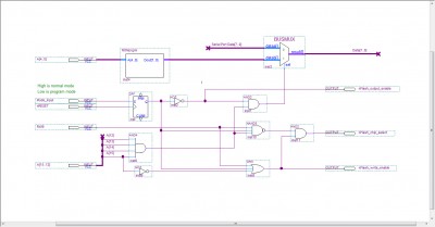
flash programmer block diagram.jpg [ 173.03 KiB | Viewed 7506 times ]


The block diagram above shows how mode influences the data path and controls of flash memory. Mode input is latched at the rising edge of nRESET. Mode latched low is the program mode that enables ROM data path in memory space $F000-$FFFF. Program mode also disables the active-low flash output enable. It also disables the active-low flash chip select unless it is a write to $8000-$FFFF.

If mode input is latched high, it is in normal mode where internal data path is disconnected from the ROM; the active-low flash output enable is always enabled; the active-low flash write enable is disabled, and the active-low flash chip select is enabled when reading memory area $F000-$FFFF.

In next session I'll describe the boot ROM and how the concept is implemented in CPLD.

Bill


Top
 Profile  
Reply with quote  
 Post subject: Re: CPLD + 6502 Trainer
PostPosted: Thu Feb 17, 2022 3:15 pm 
Offline

Joined: Fri Dec 21, 2018 1:05 am
Posts: 1076
Location: Albuquerque NM USA
Part 2 of in-situ flash programmer describes the small boot ROM in CPLD, implementation in CPLD and required engineering change.

Once the programming mode is enabled, the external flash memory is disabled and 6502 will boot from the small ROM in CPLD. This ROM is a small lookup table so not to take up too much of the limited CPLD resources. Below is the bootstrap ROM assembly source:

Code:
000000r 1               ; 2/7/22
000000r 1               ;CPLD ROM for the Flash Programmer
000000r 1               ; Put out a prompt to serial port
000000r 1               ; Load 256 bytes from serial port to $200-$2FF
000000r 1               ; Jump to $200
000000r 1               ;"Single step" switch decides whether to boot from external flash or CPLD ROM
000000r 1               
000000r 1               SerStat   = $e400
000000r 1               SerData   = $e401
000000r 1                  .org $f000
00F000  1               start:
00F000  1  A9 3C           LDA #'<'   ;put out "<" as prompt to load serial port
00F002  1  8D 01 E4        STA SerData
00F005  1  A2 00           LDX #0      ;start from $200
00F007  1               start1:
00F007  1  AD 00 E4        LDA SerStat
00F00A  1  6A              ROR A      ;look for serial data ready
00F00B  1  90 FA           BCC start1
00F00D  1  AD 01 E4     LDA SerData   ;get the data to $200+X
00F010  1  9D 00 02        STA $200,x
00F013  1  E8              INX
00F014  1  D0 F1           BNE start1   ;get 256 bytes data
00F016  1  4C 00 02        JMP $200

This small CPLD ROM program puts out a prompt and copies 256 bytes of data from serial port to RAM starting from $200-$2FF and then jump to $200. The 256-byte program is an Intel Hex file loader which, in turn, loads flash programming algorithm and the data to be programmed. This is the small CPLD ROM program as a lookup table in Verilog:
Code:
module ROMprgmr(
    input [4:0]A,
    output reg [7:0]Dout);
    always @(*)
    begin
//Boot ROM for EPROM programmer
        case(A)
     
        5'b00000: Dout = 8'ha9; // LDA #'<'   
        5'b00001: Dout = 8'h3c; //
        5'b00010: Dout = 8'h8d; // STA SerData
        5'b00011: Dout = 8'h01; //
        5'b00100: Dout = 8'he4; //
        5'b00101: Dout = 8'ha2; // LDX #0
        5'b00110: Dout = 8'h00; //
        5'b00111: Dout = 8'had; // LDA SerStat
        5'b01000: Dout = 8'h00; //     
        5'b01001: Dout = 8'he4; //
        5'b01010: Dout = 8'h6a; // ROR A
        5'b01011: Dout = 8'h90; // BCC 
        5'b01100: Dout = 8'hfa; // 
        5'b01101: Dout = 8'had; // LDA SerData
        5'b01110: Dout = 8'h01; // 
        5'b01111: Dout = 8'he4; // 
        5'b10000: Dout = 8'h9d; // STA $200,x   
        5'b10001: Dout = 8'h00; //
        5'b10010: Dout = 8'h02; // 
        5'b10011: Dout = 8'he8; // INX
        5'b10100: Dout = 8'hd0; // BNE
        5'b10101: Dout = 8'hf1; // 
        5'b10110: Dout = 8'h4c; // JMP $200
        5'b10111: Dout = 8'h00; // 
        5'b11000: Dout = 8'h02; //     
        5'b11001: Dout = 8'h00; //
        5'b11010: Dout = 8'h00; //
        5'b11011: Dout = 8'h00; // 
        5'b11100: Dout = 8'h00; // Reset
        5'b11101: Dout = 8'hf0; // 
        5'b11110: Dout = 8'h00; // 
        5'b11111: Dout = 8'h00; // 
        endcase
    end
endmodule


Attached is the schematic of CPLD. The mode latching logic, ROM data path, and external flash memory controls are similar to the block diagram described in Part 1. The external flash memory requires independent chip_select, output_enable and write_enable control signals. In current board design flash memory's chip_select and output_enable are tied together. So it is necessary to cut the trace between flash chip_select and output_enable and connect a spare output to flash output_enable. See "Cut D" and "Jumper D" of the attached picture.

I compiled and programmed the CPLD; verified it will boot from external flash in normal mode and when "Single Step" button is depressed while powering up, the console will receive a "<" prompt indicating the serial port is waiting for input. So it is ready for Part 3, loading of flash programming algorithm and data.

(BTW, it was not as simple and straightforward as the above paragraph implied--there were quite a bit of design iterations and "sailor talks" before I can write the last prargraph.)
Bill


Attachments:
Trainer_EC.jpg
Trainer_EC.jpg [ 1.33 MiB | Viewed 7463 times ]
flash programmer CPLD schematic.pdf [25.81 KiB]
Downloaded 73 times
Top
 Profile  
Reply with quote  
 Post subject: Re: CPLD + 6502 Trainer
PostPosted: Fri Feb 18, 2022 9:28 pm 
Offline

Joined: Thu Oct 05, 2017 2:04 am
Posts: 62
I developed a ROM emulator which uses a Teensy and can be programmed in C via the Arduino IDE which could be useful for your project.

https://microcorelabs.wordpress.com/202 ... -emulator/


Top
 Profile  
Reply with quote  
 Post subject: Re: CPLD + 6502 Trainer
PostPosted: Sat Feb 19, 2022 5:23 am 
Offline

Joined: Fri Dec 21, 2018 1:05 am
Posts: 1076
Location: Albuquerque NM USA
Very nice ROM emulator! I like the idea of emulators or added functions in form of 32-pin DIP or 40-pin DIP.

In this particular case the CPLD is flexible and has spare capacity so diagnostic function and/or test points can be easily added to solve a specific problem during hardware development. During ROM code development I will use scripting tool like TeraTerm Macro commands to automate file loading and flash programming so I expect the flash can be reprogrammed under 10 seconds.
Bill


Top
 Profile  
Reply with quote  
 Post subject: Re: CPLD + 6502 Trainer
PostPosted: Sun Feb 20, 2022 4:42 am 
Offline

Joined: Fri Dec 21, 2018 1:05 am
Posts: 1076
Location: Albuquerque NM USA
Part 3 of in-situ flash programmer describes the Intel Hex loader needed to load subsequent programs, algorithm for programming SST39SF0x0 and the data file.

Once the flash programmer has booted into programming mode (hold down "Single Step" button while apply power), it outputs a '<' prompt and waits for 256 bytes of binary data from the serial port. Attached is the Intel Hex loader sent to the flash programmer. This 256-byte file loader recognizes Intel Hex file and the "Gxxxx" (run from location xxxx) command. The file loader puts out a "X->" prompt when it starts up. Now I can send one or more programs and execute it. The first program is the memory diagnostic to check out the hardware as described in previous session (attached).
Attachment:
IntelHexFileLoader.zip [3.65 KiB]
Downloaded 77 times

Attachment:
MemoryDiagnosticForProgrammingMode.zip [3.47 KiB]
Downloaded 65 times

Attachment:
load RAM diag in program mode.jpg
load RAM diag in program mode.jpg [ 101.52 KiB | Viewed 7380 times ]


Now the Intel Hex loader and hardware memory are checked out, lets load the SST flash programmer attached below. The SST programmer expects a data file to be loaded in RAM from $7000-$7FFF which will be copied to $F000-$FFFF. The program implements the "Sector Erase" and "Byte Program" algorithm for SST39SF0x0. Since the flash is accessible only as write-only device, the SST program is not able to read the device's status by polling data bit7,so it just waits for the maximum specified time for erase and programming to complete; sector erase time is 25mS, max; byte program time is 20uS, max. Only sector $F000-$FFFF is erased and byte-programmed so the programming operation will complete quickly.
Attachment:
SST39SF0x0ProgrammingAlgorithm.zip [2.41 KiB]
Downloaded 70 times

Attachment:
SST39SF0x0_command_sequence.jpg
SST39SF0x0_command_sequence.jpg [ 155.75 KiB | Viewed 7380 times ]


The data file is the CPLD6502 monitor described previously (attached). It resides in flash at $F000-$FFFF but its hex file is relocated to $7000-$7FFF to be loaded in RAM at $7000-$7FFF then copied to flash at $F000-$FFFF. This is the screen shot of the programming session followed by booting the flash that was just programmed.
Attachment:
CPLD6502_monitorToBeProgrammedToFlash.zip [14.83 KiB]
Downloaded 68 times

Attachment:
flash programming session.jpg
flash programming session.jpg [ 77.41 KiB | Viewed 7380 times ]


A TeraTerm macro file to load Intel Hex loader, load SST algorithm, load data file, and program the flash is also attached. It took only few seconds to execute.
Attachment:
TeraTerm_macro_flash_programmer.zip [319 Bytes]
Downloaded 69 times


This demonstrated the flash programmer is functional and completed the project.
Bill


Top
 Profile  
Reply with quote  
 Post subject: Re: CPLD + 6502 Trainer
PostPosted: Wed Mar 02, 2022 11:43 pm 
Offline

Joined: Fri Dec 21, 2018 1:05 am
Posts: 1076
Location: Albuquerque NM USA
Atmel ATF1508AS vs Altera EPM7128S

EPM7128S is the heart of CPLD6502 trainer but it is obsolete even though it is still possible to acquire them in the secondary markets. Atmel ATF1508AS is currently in production and is the replacement with the same pin assignments and logic organization. However, ATF1508AS is more expensive, requiring a different and more expensive programmer, and using a buggy WinCUPL tool. Instead of designing with WinCUPL, it is possible to design in Quartus, convert to Atmel equivalent with POF2JED, and program with Atmel programmer. This translation process is not problem-free. In the past, specifically with 64-macrocell EPM7064S, I've had success translating simpler designs to Atmel's equivalent, ATF1504AS, but the translation failed with more complex designs. I want to try again with translation of EPM7128S to ATF1508AS, so I bought and received 3 ATF1508AS ($11 each) from Mouser. The ATDH1150USB programmer is even more expensive now at $73, but I already has purchased one.

Despite Atmel's documentation, ATDH1150USB programmer does not work with my lab computer which is Windows Vista but does work with Windows 10. The POF2JED software is easy to use and the ATMISP programming software is also reasonably easy to use. I went back to the earlier CPLD6502 designs and translate them to Atmel programming files with POF2JED. Then program Atmel ATF1508AS with ATMISP.
Attachment:
Trainer_flash_programmer_POF2JED.PNG
Trainer_flash_programmer_POF2JED.PNG [ 33.23 KiB | Viewed 7298 times ]

Attachment:
Trainer_Flash_programmer_ATMISP.PNG
Trainer_Flash_programmer_ATMISP.PNG [ 25.35 KiB | Viewed 7298 times ]


I've converted 6 CPLD6502 designs and verified ATF1508AS has the same functionalities as EPM7128S. So far ATF1508AS appears to be a viable alternative to the obsolete EPM7128S but I do notice significant higher current consumption as the complexity increases. Here are 4 current measurement of designs on CPLD6502 in order of increasing complexity:

Code:
Design      Using EPM7128S   Using ATF1508AS
1st test      115mA            123mA

7-segment
Hex display   115mA            170mA

CPLD ROM
SimpleTX   128mA            170mA

Flash
Programmer   160mA            247mA


Personally I will stay with EPM7128S until my stock run out.
Bill


Top
 Profile  
Reply with quote  
 Post subject: Re: CPLD + 6502 Trainer
PostPosted: Tue Mar 22, 2022 12:11 pm 
Offline
User avatar

Joined: Tue Aug 11, 2020 3:45 am
Posts: 311
Location: A magnetic field
I quite like this topic. It reminds me of NAND2Tetris because each step is sufficient for independent exploration. Want UART with parity? Add that yourself.

I've seen quite a few schemes where a memory map is re-arranged for flash programming. In this case, it is not required. The CPLD may selectively source reads from itself or flash storage. All writes may be directed to flash storage without restriction. Unless the magic knock sequence occurs, all writes will be ignored. Instruction fetch (or vector fetch) from flash would disrupt the knock sequence. However, if reads are exclusively from CPLD or RAM then writes to flash are not disrupted.

The current measurements for Atmel ATF1508AS are horrendous. I knew that the minimum was 105mA but I had no idea that 247mA was possible. Actually, 247mA * 5V = 1.235W. You're gonna need a heatsink on that. There might be variants which automatically fall into a low power state. I think they have a Q or Z suffix. However, they don't wake on a time-scale which is useful for address decode.

_________________
Modules | Processors | Boards | Boxes | Beep, Beep! I'm a sheep!


Top
 Profile  
Reply with quote  
Display posts from previous:  Sort by  
Post new topic Reply to topic  [ 81 posts ]  Go to page Previous  1, 2, 3, 4, 5, 6  Next

All times are UTC


Who is online

Users browsing this forum: No registered users and 2 guests


You cannot post new topics in this forum
You cannot reply to topics in this forum
You cannot edit your posts in this forum
You cannot delete your posts in this forum
You cannot post attachments in this forum

Search for:
Jump to: