6502.org Forum  Projects  Code  Documents  Tools  Forum
It is currently Thu May 09, 2024 8:45 pm

All times are UTC


Post new topic Reply to topic  [ 30 posts ]  Go to page 1, 2  Next
Author Message
PostPosted: Mon Apr 30, 2018 9:01 am 
Offline
User avatar

Joined: Thu Dec 11, 2008 1:28 pm
Posts: 10800
Location: England
Elsewhere, kakemoms asks:
kakemoms wrote:
Anyone has a link to software that stresses the 65c02 core in different ways?


Good question - other than the various test suites (specifically Klaus' suite,) when testing the PiTubeDirect models we used Elite (a game with an attract mode) and Sphere (a Basic graphics demo). But you do at least need to watch and pay attention to see if they have gone wrong, so not ideal.

We also run the ClockSp Basic benchmark, which uses a lot of Basic's facilities to report a performance figure. Not really self-checking, one can just look to see if the results are plausible - and to see that it hasn't crashed!

Any given test, when you measure it, doesn't usually cover all opcodes even, and even less likely to cover all interesting inputs. It's said, for example, that PC rollover from $7FFF to $8000 is one of the longest paths in the 6502. When testing branches, you might try to arrange worst-case address calculation, with or without a page crossing. We've found (elsewhere) that SBC of an immediate constant which is a small negative number was a worst case in one situation.

But I'd love to hear any and all suggestions from others - hence the new thread.


Last edited by BigEd on Mon Apr 30, 2018 4:31 pm, edited 1 time in total.

Top
 Profile  
Reply with quote  
PostPosted: Mon Apr 30, 2018 2:27 pm 
Offline
User avatar

Joined: Fri Dec 11, 2009 3:50 pm
Posts: 3354
Location: Ontario, Canada
BigEd wrote:
It's said, for example, that PC rollover from $7FFF to $8000 is one of the longest paths in the 6502.
BigEd wrote:
We've found (elsewhere) that SBC of an immediate constant which is a small negative number was a worst case in one situation.

These are sobering examples, and there are probably others yet to be discovered. Thanks, Ed and kakemoms, for turning our attention to this. My own interest has to do with overclocking actual CPU chips made by WDC and others, but a 65xx stress test would also be valuable for users of 65xx soft cores.

I don't necessarily advocate overclocking -- in some situations it's inappropriate or unnecessary -- but in other situations it's a perfectly viable way to reap some performance gain. I'm willing to violate published specs, particularly when it comes to WDC. The timing specs on WDC datasheets range from conservative to nonsensical/typo-ridden, and overall their credibility is almost negligible, IMO.

So, yeah -- I believe overclocking has its place, and in the previous century I built a Variable Frequency Oscillator to help in determining the limits. Basically you keep increasing the trimpot until the CPU crashes, then you back it off to allow some safety margin --- that's how you determine the operating frequency! :)

But I'm uncomfortably aware of having to guess regarding how much margin to allow. Yes there are issues of temperature variation to bear in mind, and likewise supply voltage perhaps. But the other big question mark is, what sort of code is running when these experiments are performed? So far I don't have a good answer for that -- I just try to run a piece of code that's fairly big and fairly diverse, such as the Fig Forth compiler. But it's not a very satisfactory solution. Very likely there are corner cases which don't get exercised.

-- Jeff

_________________
In 1988 my 65C02 got six new registers and 44 new full-speed instructions!
https://laughtonelectronics.com/Arcana/ ... mmary.html


Last edited by Dr Jefyll on Mon Apr 30, 2018 2:34 pm, edited 1 time in total.

Top
 Profile  
Reply with quote  
PostPosted: Mon Apr 30, 2018 2:32 pm 
Offline
User avatar

Joined: Thu Dec 11, 2008 1:28 pm
Posts: 10800
Location: England
Notably, recently revaldinho was testing a new add-on circuit for a Z80 system, and explored the margin by lowering the voltage. The other similar tactic would be to raise the temperature, but of the three, lowering the voltage and measuring the margin before the system failed might be the easiest. Having discovered the margin, you can of course then try to exploit it, perhaps by overclocking.


Top
 Profile  
Reply with quote  
PostPosted: Mon Apr 30, 2018 4:20 pm 
Offline
User avatar

Joined: Wed Mar 01, 2017 8:54 pm
Posts: 660
Location: North-Germany
Usually the stress limit of an IC is when its operation causes so much heat that the chip will get roasted sooner or later. This would be a true physical limit. Functional operation may cease earlier, but that depends on many other aspects. In the case of a CPU bus load, bus drive, propagation delays of decoders, and RAM response time do influence the behavior. So your DUT (device under test) may work fine up to 30 MHz under test bench conditions but fails at 15 MHz in its target environment.

You need to specify what exactly you want. If a complete system should work, then you have to test this system completely. If you only like to verify which of several CPUs is the fastest you could set up a test environment with exceptional fast decoding and RAM speed and then simply increase clock and voltage to get the limit. There you may check the dependency against voltage and against clock. Then define a safety margin, set conditions accordingly and run something like Klaus' test several hundred times (don't forget to check the temperatures). If it doesn't fail you can say this particular chip is capable of running at say 40 MHz @ 7 V and <100 °C. This won't help you a lot. If the target system is poorly designed, this CPU might still fail shortly beyond 8 MHz.

I don't know whether there are more or less critical opcodes, perhaps. On the other hand, is the response time of a RAM in all cases and within a byte unique or does it matter whether the previous state was same or opposite or how many address lines did change? Is the propagation delay of a decoder always constant or is there a dependency related to its previous state? How stable is the supply?

I'm still wondering why people still trying to push these old fashioned parts up to or even beyond their limits? During their times there was no other way, but today? :roll:


Top
 Profile  
Reply with quote  
PostPosted: Mon Apr 30, 2018 4:28 pm 
Offline
User avatar

Joined: Thu Dec 11, 2008 1:28 pm
Posts: 10800
Location: England
The original question was, about WDC's cores for FPGA and how fast they run, so we're in the context of stress-testing in the sense of determining the fastest correct operation in given conditions. Probably in the broader context of any and all cores for FPGAs. But that said, actual silicon also has a speed limit for internal operation, and a given system built around a chip has a speed limit too.

It's certainly true that certain combinations of opcodes, operands, machine state are going to have a lower max speed than others. And it's true that a given program, even Klaus' testsuite, doesn't even use all operations with all addressing modes and all operands and all machine state. Even Wolfgang Lorenz' doesn't do that. So if you do run a given program, and find the maximum speed, that will be the maximum speed for that program (and that specific chip) but is probably not the maximum speed for every program.

So, it's an art, and an imperfect art, to try to find the speed of a CPU. Still, the better your test, the closer your answer is to the truth, and the less margin you might feel you need to apply.

As for why, as ever, on this forum that doesn't seem like a great question to ask - each of us has our reasons for doing what we do. All you might say is that you don't feel a need to look into this.


Top
 Profile  
Reply with quote  
PostPosted: Mon Apr 30, 2018 4:57 pm 
Offline
User avatar

Joined: Wed Mar 01, 2017 8:54 pm
Posts: 660
Location: North-Germany
The design tools for FPGAs usually report the longest or most critical path and its delay. Most likely their is already a safety margin included and the calculation might not be exact. But under this circumstances you could try to add or change a path so it becomes exceptionally long and slow. Then you might test exactly this path by using the correspondent instruction and look how far you come.


Top
 Profile  
Reply with quote  
PostPosted: Wed May 02, 2018 10:23 pm 
Offline

Joined: Wed Mar 02, 2016 12:00 pm
Posts: 343
The software suite that follows a FPGA, tend to look for propagation delays. It assumes that a signal that is used within a clocked module has to reach its state before that clock triggers. That is somewhat indicative on how slow you have to drive a circuit to be on the safe side, but not always will it correspond to how fast you can drive it.

This is certainly more due to design, so that a certain design can withstand more slack with these timings than others. Then you also have to consider production, ic and packaging variations, which is all baked into the above mentioned propagation delay.

So if your software suite says 25MHz, that is certainly worst case all considered, and it would be interesting to stress that speed with a stress-test program that does try to run all kinds of instructions in different given patterns. Or as Big Ed says, in any thinkable or unthinkable combination.


Top
 Profile  
Reply with quote  
PostPosted: Thu May 03, 2018 5:02 am 
Offline
User avatar

Joined: Thu Dec 11, 2008 1:28 pm
Posts: 10800
Location: England
The most important thing for most people, and for the FPGA vendor, is that an implementation which is supposed to work at (say) 50MHz, does work at that speed. So the timing analysis should always be conservative - reliability and repeatability are very important.

That said, even with temperature and voltage reasonably in-spec, I think we've often seen that there's not much scope for over-clocking. It might be relevant that on FPGA the critical path often includes a lot of "routing" delay: the logic being only a minor part of the clock cycle, transporting the signal from one part of the chip to another being a major part. On a commercial custom CPU, that's less true, because a huge amount of effort goes into making the CPU design fast, which means making every logic gate count. (Moving data between two cores, or from CPUs to peripherals on-chip, can still take substantial time, let alone moving data on or off chip.)


Top
 Profile  
Reply with quote  
PostPosted: Sun Jul 01, 2018 9:31 am 
Offline

Joined: Wed Mar 02, 2016 12:00 pm
Posts: 343
Just to follow this up a bit:

For new circuits, one either uses a IC or a soft core. For the hard core, the combination of different parts can lead to whatever, and a stress test will show how stable a certain combination is. No overclocking required to make a system fail!

For FPGA soft cores, the design and more critically; the implemented circuit can give very different results under different circumstances. Specifically a full vs a scarsely populated FPGA will yield very different with respect to optimal routing and time-delays. If you get above 70-80% usage of a particular asset (Slices, RAM, LUTS), the routing becomes difficult and you will get much more unstable results. The reported speed may be the same, but the actual result will not(!).

In either case a stress-test suite is important. That we can trust the numbers given by any software or manufacturer without properly stress-testing is a dubious assumption. Temperature also has to be taken into the equation, so a proper testing should at least be done at two or more temperatures (high/low/normal range). The time involved is also important as a semi-stable system can show a glitch after 20 minutes of operation. In fact, I had such a problem once in which running 20 minutes with INC instructions gave several glitches, while it was stable without the INC(!)

For a hobby breadboard computer I wouldn't care at all about such testing, but if you want to sell the lot, such an exercise will certainly reduce your headache.


Top
 Profile  
Reply with quote  
PostPosted: Sat Aug 25, 2018 1:43 am 
Offline

Joined: Thu Aug 23, 2018 7:10 am
Posts: 89
Location: CyberBunker
we just use a full memory test for that. but then again we don't want to check if all the instructions work, we just wanna know the -boards- are stable... but then again... even when it's just looping it's irq vector to a cli and a brk or doing a jmp to self a 6502 will always be equally 'busy'. i think a real stresstest would involve having the maximum load on all of it's i/o pins (or more) and running at either -40, 0 or 85 or 125C for a month or 3 and have not so much to do with what code it is executing. (as -any- instruction results in bus operations. there is no 'cache' ;) (figured that one out as the memory test initially read some other known value each time from a different location to fix impedance if a chip wasn't present at all, under which conditions sometimes a system reports the last value written to the bus (the same location) due to the capacitance on the bus... bbbbutttt on 6502's the bus is automatically cleared as after the STA... it actually loads the LDA from the rom, resetting both the data and the address bus in case there ever was any capacitance 'leftovers' on the databus due to everything but the cpu being in high-z state ;) there literally is -no cache-. even nops and jumps to self get constantly read. everything results in bus accessess. maybe the only thing that matters is how many pins it simultaniously has to drive high so LDA #$FF ; STA $FFFF (24 pins 1) would probably make more amperes go through the 6502 than LDA #$00 ; STA $0000 (24 pins 0) in an endless loop. especially when the bus is fitted with a bunch of resistors to ground to the maximum specified load (or more)


Top
 Profile  
Reply with quote  
PostPosted: Sat Aug 25, 2018 1:52 am 
Offline

Joined: Thu Aug 23, 2018 7:10 am
Posts: 89
Location: CyberBunker
emulators and fpga designs however need a different type of stress test, one in which every single opcode is executed with every possible parameter, registers, and flags set in advance and each time the result and all flags and all supposedly unaffected other registers are checked. probably better done by hooking them up to an external computer system simulating the rest of the board and feeding them instructions rather than have them execute their own self-test. also the number of cpu cycles timing in case one wants to keep that 'compatible' to nmos 6502s (although other than for emulating legacy systems, i would not know why the hell one would want to keep the number of cpu cycles exactly the same as on let's say a c64 on systems you're gonna run at 200mhz or so anyway and therefore by definition are not 'timing compatible' at all ;)
as for 'undocumented/illegal opcodes' well. people should not have used those in their code anyway. it's not your fpga or emulator that's broken. it's their software. :P


Top
 Profile  
Reply with quote  
PostPosted: Sat Aug 25, 2018 2:06 am 
Offline

Joined: Thu Aug 23, 2018 7:10 am
Posts: 89
Location: CyberBunker
GaBuZoMeu wrote:
I'm still wondering why people still trying to push these old fashioned parts up to or even beyond their limits? During their times there was no other way, but today? :roll:


During their days (1976'ish) you could just buy a pdp-11 or an ibm (not the small ones, the big ones ;) or one of those big-ass trs-80 things that came with a desk attached and a bunch of 8" floppy drives. there never was any 'need' to 'push parts up to their limits' and neither is there now in the pc world (they can just go and buy an ibm power7 system which will happily run at 4ghz or 5ghz per core, which is roughly twice what a single core in a pc will do ;) (and guess what, they're cheaper than xeons ;) hell they can buy a few racks full of them and build a supercomputer out of them :P

if you need to 'push parts to their limits' you got the wrong computer for the job, or you didn't buy enough computers to do the job within an acceptable time.

but. systems do need to be tested as part of normal product development. so you build like 10 of them and make them run in the oven, in the fridge, underwater, on the moon, while exposed to radioactive particles, next to a 10 megawatt tv transmitter, whatever driving full load and more. normally you make 1500 of them and see how many % of them failed within how much time.

also the signals should remain nice and square'ish on the scope and not turn into spikes. stuff should not broadcast radio while it's doing it's job, it also should not use the wall outlet as an extension of it's databus leaking data onto either the electricity network or it's ground connector (ps/2 keyboards much? ;) 
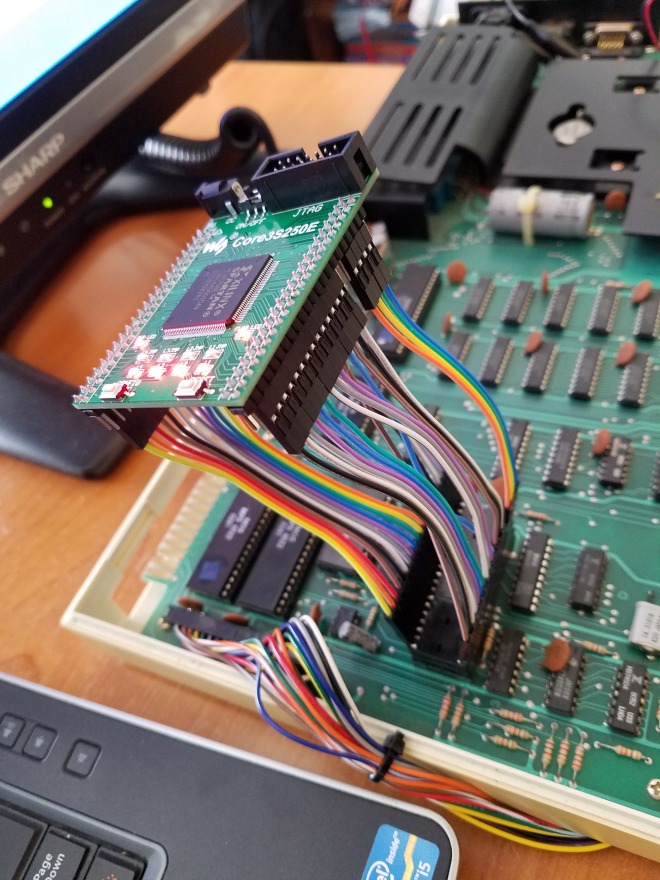
etc. this is where the 'testing' part comes in. it's not about 'seeing how fast it will go' it's about seeing if it's good enough not to crap up on you halfway through. also the 65c02 and 65c816 are not 'old fashioned parts' they do the job. they are proven to do the job and nothing but the job. are 'lightswitches' old fashioned parts?, drills, definately old fashioned parts. lasers are far cooler. steeringwheels, gas pedals and brakes in cars, not to mention stick shifters, 'old fashioned parts' you could after all use a nifty joystick or a 'touchscreen' running that android garbage :P (now don't give car manufacturers any more retarded ideas than they already recently got ;)

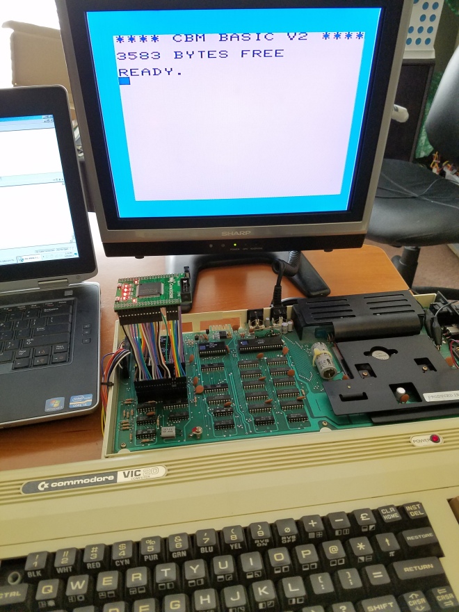
6502's weren't the height of technology and speed when they came out. the whole 'microcomputer revolution' which they caused was more of a side effect but they never were the ultimum in cpu power, ever. they were cheap, multivendor, reliable, easy to implement, and got the job done. and they still are all of that today. if it was a somewhat 'larger' job you wanted done you would not buy a 6502 based system, even in 1976. we had a kim-1 at home somewhere around that time, shortly before the first ibm pc came around, but also stacks of punch cards for an ibm mainframe. which is how the real work was done. punching cards with a manual tool and flow charts on paper. nuff said on that. :P you don't take a 6502 to run the accounting of your bank on now do you :P hate to break it to all those 'my zx spectrum is better than your c64' people but neither of them even were 'high tech' even on the day they came out. they did have fancy colors and sounds tho :P but even in those fields one could buy better systems. the average video arcade cabinet of those days by far has better capabilities for that. consumer stuff will always be a decade behind the real stuff. now. as for the 6502. it was meant to compete with the motorola 6800. so it was meant for industrial control applications straight from the start and that pretty much is the thing it does best and still does today and probably still will do 40 years from now.


Top
 Profile  
Reply with quote  
PostPosted: Sat Aug 25, 2018 2:40 am 
Offline

Joined: Mon Mar 02, 2009 7:27 pm
Posts: 3258
Location: NC, USA
In regards to the heat stress test an IC has to go through in order to pass an (I)ndustrial IC rating is way more than a (C)ommercial rating. Recently ordered some Xilinx Spartan 6 (I) grade and they are spec'd for automotive use, which is one step above Commercial grade. MIL-Spec is one grade above even the (I) spec. Then I'm sure you've got your Rad-hard spec for outer space stuff. 1802 anyone?

Sorry none of this info helps the OP. :(

_________________
65Org16:https://github.com/ElEctric-EyE/verilog-6502


Top
 Profile  
Reply with quote  
PostPosted: Sat Aug 25, 2018 6:35 pm 
Offline

Joined: Thu Oct 05, 2017 2:04 am
Posts: 62
I think a good way to check the correctness of your 6502 core is to hook it up to a vintage machine and run as much software as you can. You are more likely to experience a greater variety of opcode combinations than you would with small assembler testing programs. It also allows you to see if your implementation is speed compatible if that is your goal. Otherwise you could try to create the "World's Fastest xxx" by running your core at max speed.

You could use bus converters to translate between 5V and 3.3V to preserve your FPGA's IOs, or you can simply hook it directly to a "disposable" $20 board and enjoy it as long as it lasts. (Mine still works without any blown IOs.)

Image

Image


Top
 Profile  
Reply with quote  
PostPosted: Sat Aug 25, 2018 10:07 pm 
Offline
User avatar

Joined: Wed Mar 01, 2017 8:54 pm
Posts: 660
Location: North-Germany
Me thinks the discussions diverts into two distinct directions.
Direction 1 deals with the question whether or not a core behaves exactly like an original device.
Direction 2 deals with the question of how far - in terms of speed or clock frequency - a given device (not necessarily an FPGA) can be driven and what safety margins exists when the clock frequency is lowered.

IMO direction 1 is only verifiable by running as much given software as possible. A positive result is never fully achievable as there might be some piece of software anywhere that behaves different in relation to the reference. But the more software is checked the more likely the emulation is proper.

In theory one could do a 1:1 comparison between the emulated and the original device by means of a couple of comparators. Driving the emulated and the original device with the same signals all output signals should be identical as well. There may be slight variations tolerable like rise and fall times of edges or voltage levels as long as all signals meet the requirements within the given frame. (E.g. valid data is stable xx ns before and yy ns after the falling edge of PHI2 in case of a write cycle.) One could then tryout all instructions with various data at various addresses to seek for differences. The problem is - similar to just running given SW - will really all important variants be verified? Thinking about the indirect jump address fetch error of the old NMOS 6502 I believe NO, any synthetic test won't cover all possible combinations that exist.

Direction 2 deals with the problem of safety margins. To check how far one can go in terms of clock speed (assuming the surrounding components are superior) is easy. Just using a VCO or something similar and increase the frequency until the system runs into errors. The used software during this test should cover all instructions in all special cases (with and without page crossings, decimal mode, all address regions if possible). Of course the working conditions should be stable. That is a constant supply voltage and a (nearly) constant case temperature.

For CMOS devices I assume that the following relations between propagation delay, supply voltage, and temperature are still valid, although these specs are taken from the SYNERTEK cell library from (SYNERTEK DATA BOOK 1985):
Attachment:
PrDLYvsVdd.png
PrDLYvsVdd.png [ 5.35 MiB | Viewed 3707 times ]

Attachment:
PrDLYvsTMP.png
PrDLYvsTMP.png [ 4.91 MiB | Viewed 3707 times ]

Attachment:
PDvsVdd.png
PDvsVdd.png [ 5.13 MiB | Viewed 3707 times ]


The relations shown in the graphs seems logical from a physical point of view. Higher temperatures will increase the drain-source resistances causing slower dis/charge of next gate caps increasing the prop delay. Rising voltages increase the gate drive, lowering the DS resistance, reducing the prop delay. What is unknown is the how strong the effect of these variations is. These graphs may be a starting point for verifications of a given device.


Regards
Arne


Top
 Profile  
Reply with quote  
Display posts from previous:  Sort by  
Post new topic Reply to topic  [ 30 posts ]  Go to page 1, 2  Next

All times are UTC


Who is online

Users browsing this forum: No registered users and 6 guests


You cannot post new topics in this forum
You cannot reply to topics in this forum
You cannot edit your posts in this forum
You cannot delete your posts in this forum
You cannot post attachments in this forum

Search for:
Jump to: