This is for BigD (although of course anyone can comment/ask questions) who I think asked about the CPLD in my 6502gpd 2.1 design and if the memory map works in WinSim (WinCUPL's simulator). It does and also works when I test the design in the flash (so to speak).
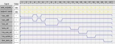
WinSim:
Signals:
Addr_msb[7..0] = A15-A0 of the 65c02 address bus
Bnk[3..0] = Bank latch output. Selects bank 0 to 15. inputs connected to D3-0 of the 65c02 data bus
!ram_selA = ram IC A select (banks 0-7). active low.
!ram_selB = ram IC B select (banks 8-15). active low.
!rom_sel = rom select. active low.
!acia_sel = serial/acia select. active low.
!via_user_sel = user VIA select. active low.
!via_system_sel = system VIA select. active low.
!bnk_latch_sel = bank latch select. active low.
Bank latch:
There are 16 banks (0-15) with each bank comprising 64KB of RAM. Not all of this is used as certain memory ranges don't map to ram or they map to only bank 0 ram.
Writing a 4 bit number to $9f00 will write to the latch and so change the bank to that.
RAM ICs:
Each RAM IC is 512KBx8 for a total of 1024KB. Banks 0-7 map to the first IC (ramicA) and banks 8-15 map to the second one (ramicB).
Each ram IC has address pins A0-A18. A0-15 is linked to the 65c02 address bus, A16-18 is determined by the CPLD (ATF1504AS) which in turn depends on the bank address.
Memory map:
Code:
0000-0FFF : Always maps to bank 0 RAM, irrespective of bank address
1000-8FFF : Mapps to RAM, bank address latch determines which IC and address range is used within it
9000-90FF : (Not mapped)
9100-91FF : ACIA/Serial IC selected irrespective of bank address
9200-92FF : User VIA IC selected irrespective of bank address
9300-93FF : System VIA IC selected irrespective of bank address
9400-9EFF : (Not mapped, for future expansion)
9F00-9FFF : Bank address latch. IC selected irrespective of bank address. Write only.
A000-DFFF : If bank 0 selected then ROM selected, otherwise works the same as 1000-8FFF range
E000-FFFF : Always maps to ROM, irrespective of bank address
Here's the output of WinSim (let me know if you need me to change the colours):
Attachment:
 Simulator.JPG [ 54.85 KiB | Viewed 616 times ]
Here are the signals from the SI file used to generate the above (I've added comments next to each line for this post):
Code:
ORDER: addr_msb7..addr_msb0, bnk3..bnk0, !ram_selA, !ram_selB, !rom_sel, !acia_sel, !via_user_sel, !via_system_sel, !bnk_latch_en;
VECTORS:
'00' '0' ******* // address: 0000, bank 0, expected: ram_selA
'00' '8' ******* // address: 0000, bank 8, expected: ram_selA
'10' '0' ******* // address: 1000, bank 0, expected: ram_selA
'10' '8' ******* // address: 1000, bank 8, expected: ram_selB
'4F' '0' ******* // address: 4f00, bank 0, expected: ram_selA
'4F' '8' ******* // address: 4f00, bank 8, expected: ram_selB
'F0' '0' ******* // address: f000, bank 0, expected: rom_sel
'F0' '8' ******* // address: f000, bank 8, expected: rom_sel
'D0' '0' ******* // address: d000, bank 0, expected: rom_sel
'D0' '8' ******* // address: d000, bank 8, expected: ram_selB
'90' '0' ******* // address: 9000, bank 0, expected: Nothing selected
'90' '8' ******* // address: 9000, bank 8, expected: Nothing selected
'91' '0' ******* // address: 9100, bank 0, expected: acia_sel
'91' '8' ******* // address: 9100, bank 8, expected: acia_sel
'92' '0' ******* // address: 9200, bank 0, expected: via_user_sel
'92' '8' ******* // address: 9200, bank 8, expected: via_user_sel
'93' '0' ******* // address: 9300, bank 0, expected: via_system_sel
'93' '8' ******* // address: 9300, bank 8, expected: via_system_sel
'94' '0' ******* // address: 9400, bank 0, expected: Nothing selected
'94' '8' ******* // address: 9400, bank 8, expected: Nothing selected
'9F' '0' ******* // address: 9f00, bank 0, expected: bnk_latch_sel
'9F' '8' ******* // address: 9f00, bank 8, expected: bnk_latch_sel


