6502.org Forum  Projects  Code  Documents  Tools  Forum
It is currently Sun May 12, 2024 5:20 pm

All times are UTC


Post new topic Reply to topic  [ 28 posts ]  Go to page Previous  1, 2
Author Message
PostPosted: Mon May 30, 2016 8:16 pm 
Offline
User avatar

Joined: Fri Aug 30, 2002 1:09 am
Posts: 8433
Location: Southern California
I like the distributed grounds. +5V bypassed to ground would qualify for purposes of good AC performance too. As far as routing the 96-pin connector goes, there's no problem getting two traces per layer between pins of row C (the row farthest from the edge of the board); so I don't think you need to worry about having any difficulty at all routing the 96-pin. You might even be able to get three traces between pins; but it won't be necessary. I think every board house around will do .006"/.006" trace/space before charging extra. Some can make the trace as narrow as its thickness, so it has a square cross section. How they can do that is beyond me, but I've seen photomicrographs of it. You can also get WW 96-pin DINs (which I'm using).

_________________
http://WilsonMinesCo.com/ lots of 6502 resources
The "second front page" is http://wilsonminesco.com/links.html .
What's an additional VIA among friends, anyhow?


Top
 Profile  
Reply with quote  
PostPosted: Mon May 30, 2016 10:21 pm 
Offline

Joined: Sat Jan 04, 2003 10:03 pm
Posts: 1706
My PCB layout software complained of DRC violations when I tried putting two traces between row C pads. Maybe there is a setting I can tweak, or maybe the footprint uses pads which are bigger than what you use.


Top
 Profile  
Reply with quote  
PostPosted: Tue May 31, 2016 12:11 am 
Offline
User avatar

Joined: Fri Aug 30, 2002 1:09 am
Posts: 8433
Location: Southern California
For most things, I use pads that are only .020" greater diameter than the finished hole. So for example thru-hole ICs' pads are usually .050" diameter with .030" hole, leaving .050" between pads which allows getting two traces in between pads using .010" trace and space, or three three traces in between pads if minimum trace & space are .006" or .007". For .025" square posts (like pin headers), I use a .040" hole and .060" pad, leaving .040" in between, which still allows two traces through if minimum trace and space is .008" or less. I'm always watching the X-Y display, frequently use the calculator to get things spaced right rather than rely on eyeballing something, and I don't use snap-to-grid (unless .001" is considered a grid).

_________________
http://WilsonMinesCo.com/ lots of 6502 resources
The "second front page" is http://wilsonminesco.com/links.html .
What's an additional VIA among friends, anyhow?


Top
 Profile  
Reply with quote  
PostPosted: Fri Jun 03, 2016 3:07 am 
Offline

Joined: Sat Jan 04, 2003 10:03 pm
Posts: 1706
Well, thanks to the advice from Garth on how to pack things in between the pins of the DIN connector, I finally ended up with a PCB layout like so: Image

This is, of course, just a preview of what the finished board would look like. The reverse side is boring: just a grounded copper fill with a few necessary traces to avoid jumpers on the top-side.

The power supply section is in need of manual rework; I think some of the traces are too small. Not that it matters for my immediate needs (I'm just driving two LV-TTL chips), but I think some of those traces should be thickened and re-routed by hand. It's the only section that I used auto-routing on, and that was only to clean up the display while I hand-routed the DIN connectors and TTL logic.


Top
 Profile  
Reply with quote  
PostPosted: Fri Jun 03, 2016 11:07 pm 
Offline
User avatar

Joined: Fri Dec 11, 2009 3:50 pm
Posts: 3354
Location: Ontario, Canada
Hi Sam -- nice PCB! :) Reminder, though: It's a bit easier (and better) if you attach images to your posts, rather than hosting 'em off-site.

kc5tja wrote:
Well, thanks to the advice from Garth on how to pack things in between the pins of the DIN connector, I finally ended up with a PCB layout like so: [...] This is, of course, just a preview of what the finished board would look like.
Hmm, maybe you already noticed, but it seems that, for the final version, those zig-zags could advantageously be moved a bit -- horizontally I mean. (Original and modified motifs shown below.) It's just a suggestion; I realize the Design Rules may be satisfied as-is.
Attachment:
pcb mod.png
pcb mod.png [ 20.46 KiB | Viewed 3996 times ]

kc5tja wrote:
The reverse side is boring: just a grounded copper fill with a few necessary traces to avoid jumpers on the top-side.
Is the back side intended to act as a ground plane, then? Connector pins that're grounded attach to it? (Just asking. I hope those traces you mentioned are short.)

cheers
Jeff

_________________
In 1988 my 65C02 got six new registers and 44 new full-speed instructions!
https://laughtonelectronics.com/Arcana/ ... mmary.html


Top
 Profile  
Reply with quote  
PostPosted: Sat Jun 04, 2016 12:19 am 
Offline
User avatar

Joined: Fri Aug 30, 2002 1:09 am
Posts: 8433
Location: Southern California
Yes, I started writing Thursday night, then put it aside, thinking what I wrote sounded too picky. I'm sure it'll work as is, and it does look nice so don't let this come across as negative.
_________________

Wow, it sure looks like you already got boards made; but how could it be so fast? It looks nice.

If that's just a super good simulated picture and they're not made yet, I'd say you could further improve the spacing between traces and pads by removing the lock to 45-degree increments so you can use any angle, then come out of every row-A and row-C pin away from the connector at nearly 0 degrees instead of 45, and making the traces spaced more equidistant rather than grouped in threes. If the rise times are fast enough to matter, you'll get less cross-coupling between traces if their separation, relative to the distance to the ground plane (which in this case is the thickness of the board), is increased.

Related, for my next picky point, I notice in Jeff's second picture that the traces come to pads with angles of less than 90 degrees. I would make it so the last segment of each trace heads straight for the center of the pad. PCB manufacture seems to have improved enough over the years that it may not be a problem anymore, but the smaller angles tended to be harder to wash the chemicals out of in the manufacturing process, leading to problems in long-term reliability. I still try to have no angles of less than 90 degrees.

_________________
http://WilsonMinesCo.com/ lots of 6502 resources
The "second front page" is http://wilsonminesco.com/links.html .
What's an additional VIA among friends, anyhow?


Top
 Profile  
Reply with quote  
PostPosted: Sat Jun 04, 2016 6:00 am 
Offline

Joined: Sat Jan 04, 2003 10:03 pm
Posts: 1706
GARTHWILSON wrote:
Wow, it sure looks like you already got boards made; but how could it be so fast? It looks nice.


It's a simulation, rendered by the PCB tool. It's also a fairly low resolution render too; some traces come very close or even overlap with some pads in the simulation, but they meet DRC rules in the actual gerbers.

Quote:
If that's just a super good simulated picture and they're not made yet, I'd say you could further improve the spacing between traces and pads by removing the lock to 45-degree increments so you can use any angle, then come out of every row-A and row-C pin away from the connector at nearly 0 degrees instead of 45, and making the traces spaced more equidistant rather than grouped in threes.


I tried it originally, and it results in traces for even numbered slots overlapping traces for odd-numbered slots. I even tried alternating side-to-side, and I still get the same problem. The only way they'll all fit is if I bunch them up like that.

That said, the center trace is either ground or +5V, and the reverse side is a ground plane, so I'm hoping that will compensate for this design.

Quote:
If the rise times are fast enough to matter


And they will be; I'm working with FPGAs with I/O pins capable of 250MHz or faster rates, remember. ;)


Top
 Profile  
Reply with quote  
PostPosted: Sat Jun 04, 2016 6:15 am 
Offline
User avatar

Joined: Fri Aug 30, 2002 1:09 am
Posts: 8433
Location: Southern California
I'd like to do a layout to illustrate what I mean, but don't wait for me. It may be a while before I can get to it. I still need to do some tests on undocumented '816 behavior details for one of our newest members too, since I have my tester set up and offered.

I believe the standard panels for 3U boards for a VME card cage are made for the slots to be 0.800" on centers. If that's of any interest to you, it might be good to space yours accordingly. You don't have to use panels, or use stock panel blanks.

Attachment:
NIcardcage.jpg
NIcardcage.jpg [ 37.2 KiB | Viewed 3983 times ]

_________________
http://WilsonMinesCo.com/ lots of 6502 resources
The "second front page" is http://wilsonminesco.com/links.html .
What's an additional VIA among friends, anyhow?


Top
 Profile  
Reply with quote  
PostPosted: Sat Jun 04, 2016 7:24 am 
Offline

Joined: Sat Jan 04, 2003 10:03 pm
Posts: 1706
My slots are spaced at 1.0" centers for easier access to the bus-grant jumpers and perhaps for sticking o'scope probes inside.

This backplane is not intended to sit in a rack, nor is it VME compatible. Its purpose is to let me break the Kestrel-3 into different components, so I can work on them in isolation. Once everything is done (where done is defined as, "I have a working computer with working video display and keyboard input"), I'd like to place everything onto a single board.

Is there a reason for recommending 0.8" centers, other than compatibility with existing card cage chassis?


Top
 Profile  
Reply with quote  
PostPosted: Sat Jun 04, 2016 7:53 am 
Offline
User avatar

Joined: Fri Aug 30, 2002 1:09 am
Posts: 8433
Location: Southern California
kc5tja wrote:
Is there a reason for recommending 0.8" centers, other than compatibility with existing card cage chassis?

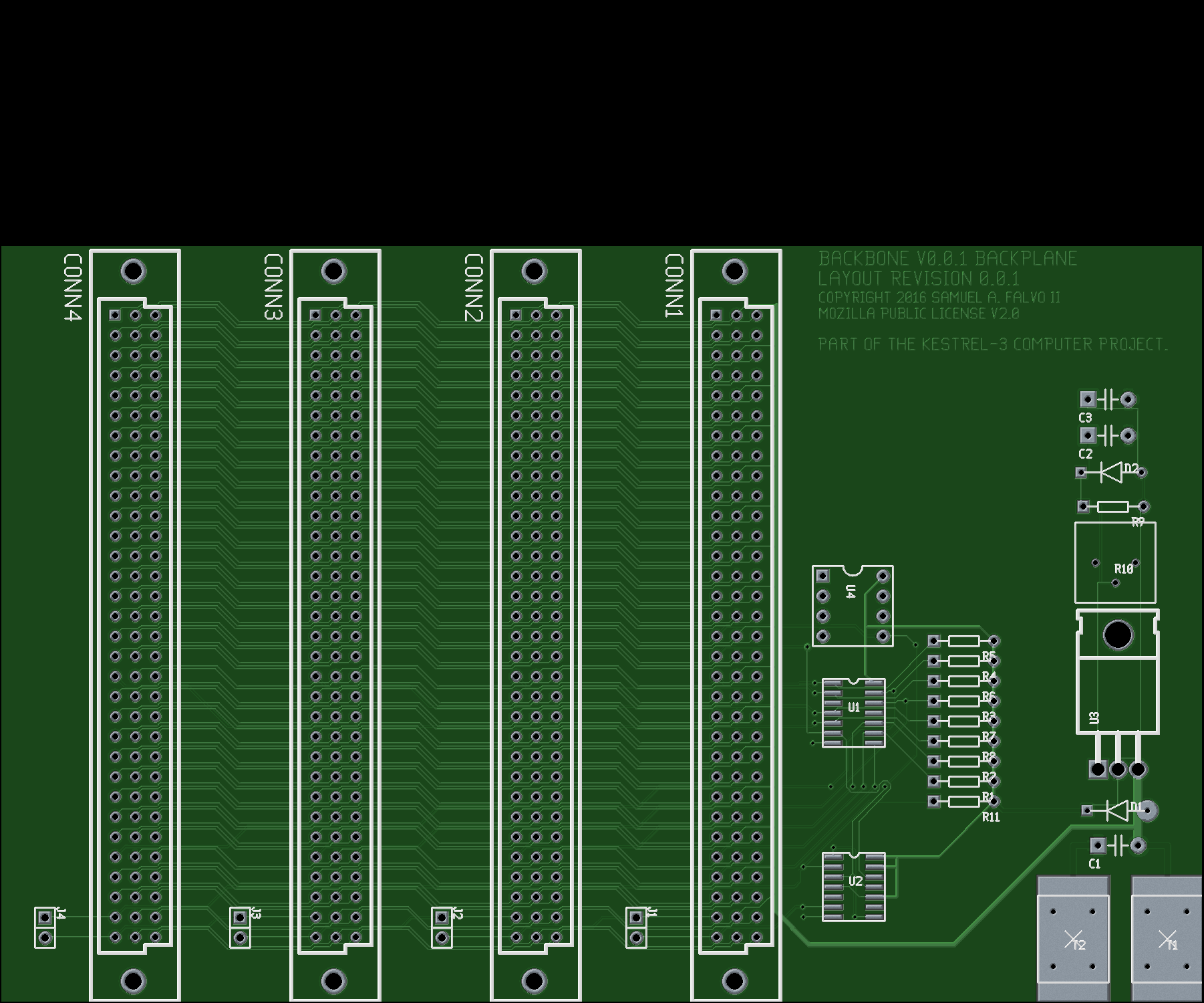
Not really. I have my slots at 2x(0.8") intervals, ie, 1.6", so I could use double-width standard panel blanks if I decide to, and I'll have plenty of room between for WW boards. (I have the 96-pin DIN connectors in WW too.) My card cage is only half rack width, but I don't anticipate ever putting more than three or four cards in it, so I can have plenty of room to put even 3.2" (minus board thickness) between the surfaces of two boards if necessary for probing without extension cards, for debugging. The card cage has removable top and bottom panels, so you can reach in for probing or for plugging in more things.

Here's the portable rack, standing on end, looking at the bottom. The perforated top and bottom panels come out. The card guides snap in and out easily. The front panel will hold the LCD and keypad. It is on hinges, and is held down with thumbscrews during transport to protect things.
Attachment:
RackBottom.jpg
RackBottom.jpg [ 59.74 KiB | Viewed 3974 times ]


Here the panel is hinged up where it sits at an angle:
Attachment:
RackFront.jpg
RackFront.jpg [ 74.15 KiB | Viewed 3974 times ]


Here's the back, open, before I wired up the backplane (which the processor's own buses will not go out on) and before I added the battery holders for portable operation and connectors in the back for external power, RS-232 ports, printer port, external speaker, and reset button:
Attachment:
RackBackOpen.jpg
RackBackOpen.jpg [ 66.98 KiB | Viewed 3974 times ]


...and closed, again before I added connectors and reset button:
Attachment:
RackBackClosed.jpg
RackBackClosed.jpg [ 41.81 KiB | Viewed 3974 times ]


I'll get some more-updated pictures later.

_________________
http://WilsonMinesCo.com/ lots of 6502 resources
The "second front page" is http://wilsonminesco.com/links.html .
What's an additional VIA among friends, anyhow?


Top
 Profile  
Reply with quote  
PostPosted: Sun Jun 05, 2016 6:29 am 
Offline

Joined: Sat Jan 04, 2003 10:03 pm
Posts: 1706
Putting the slots at 1.6" centers would roughly double the cost of the board (doubles the surface area), and would lead to traces >4", thus requiring termination (instead of it being merely a recommendation). Also, card cages seem to be optimized for 100mm x 160mm Eurocards. I'm looking "cards" that are closer to 3.5" x 1.5" in size (give or take space needed for external ports). Again, looking to RC2014 computer for inspiration. The backplane is intended to carry the main CPU bus.


Top
 Profile  
Reply with quote  
PostPosted: Sat Jun 11, 2016 11:32 pm 
Offline

Joined: Sat Jan 04, 2003 10:03 pm
Posts: 1706
Fixed last known batch of bugs in the PCB layout, and I've now placed an order. Here's hoping everything works when I put it all together.


Top
 Profile  
Reply with quote  
PostPosted: Thu Aug 17, 2017 12:45 am 
Offline
User avatar

Joined: Fri Aug 30, 2002 1:09 am
Posts: 8433
Location: Southern California
We were talking about diode terminations on page 1 of this topic. I came across this ap. note from what used to be National Semiconductor (then Fairchild, now ON Semiconductor), regarding taking advantage of the static-protection diodes that are built into most CMOS ICs: https://www.onsemi.com/pub/Collateral/AN-610-D.PDF, "Terminations for Advanced CMOS Logic." It says in the first part under the "No Termination" heading,

    Clamp diodes at the inputs of most logic devices tend to reduce the ringing and over-shoots. Often, these clamp diodes are sufficient to insure reliable system operation.

In their note 393 at https://www.onsemi.com/pub/Collateral/AN-393-D.PDF, "Transmission-Line Effects Influence High-Speed CMOS," it says in the 3rd paragraph,

    Furthermore, controlling unwanted reflections is easier in the CMOS designs, because 54HC/74HC devices’ electrostatic-protection diodes tend to clamp the reflected voltages to the power-supply levels.

and later on,

    Also, the input of a 54HC/74HC gates has diodes to Vcc and ground; these diodes clamp the reflected signal as it tries to exceed the supply level.

_________________
http://WilsonMinesCo.com/ lots of 6502 resources
The "second front page" is http://wilsonminesco.com/links.html .
What's an additional VIA among friends, anyhow?


Top
 Profile  
Reply with quote  
Display posts from previous:  Sort by  
Post new topic Reply to topic  [ 28 posts ]  Go to page Previous  1, 2

All times are UTC


Who is online

Users browsing this forum: No registered users and 7 guests


You cannot post new topics in this forum
You cannot reply to topics in this forum
You cannot edit your posts in this forum
You cannot delete your posts in this forum
You cannot post attachments in this forum

Search for:
Jump to: