6502.org Forum  Projects  Code  Documents  Tools  Forum
It is currently Mon Jun 03, 2024 3:44 pm

All times are UTC


Post new topic Reply to topic  [ 27 posts ]  Go to page Previous  1, 2
Author Message
PostPosted: Fri Feb 20, 2015 3:35 pm 
Offline

Joined: Mon Nov 11, 2002 6:53 pm
Posts: 79
Location: Seattle
The one thing I like about CPLD's is the fact that they don't have to be configured on boot. One thing to note though is that 'most' CPLD's only have a re-write span of 100 times or so.

With regards to the limited #of resources / pins, I actually see that as a challenge! Kinda like doing 3d code on a 6502! It's amazing how much you can do when you give it some though. I managed to put a VGA controller, DMA engine and all the glue logic (address decoding, registers etc) into a single EPM7128. In this particular case, the main clock was 25mhz, divided down twice: Once for driving a 256x192 display (80ns access time) and then again for the CPU. The DMA engine had a separate bus to VRAM and a fixed, interleaved read/write cycle with a temporary hold register that stored 2 pixels in order to allow the DMA to perform a read or write.

Anyway, keep us posted on your design!

Yvo


Top
 Profile  
Reply with quote  
PostPosted: Fri Feb 20, 2015 6:04 pm 
Offline
User avatar

Joined: Thu May 28, 2009 9:46 pm
Posts: 8198
Location: Midwestern USA
yzoer wrote:
The one thing I like about CPLD's is the fact that they don't have to be configured on boot. One thing to note though is that 'most' CPLD's only have a re-write span of 100 times or so.

I took a quick look at Atmel's ATF1508AS data sheet and noted that the part is good for 10,000 erase/program cycles.

_________________
x86?  We ain't got no x86.  We don't NEED no stinking x86!


Top
 Profile  
Reply with quote  
PostPosted: Fri Feb 20, 2015 11:19 pm 
Offline

Joined: Mon Aug 05, 2013 10:43 pm
Posts: 258
Location: Southampton, UK
yzoer wrote:
The one thing I like about CPLD's is the fact that they don't have to be configured on boot. One thing to note though is that 'most' CPLD's only have a re-write span of 100 times or so.


Yes, the separate config flash, and delay time before the circuit is useable, are two disadvantages of FPGAs.

Quote:
With regards to the limited #of resources / pins, I actually see that as a challenge! Kinda like doing 3d code on a 6502! It's amazing how much you can do when you give it some though. I managed to put a VGA controller, DMA engine and all the glue logic (address decoding, registers etc) into a single EPM7128...


Ok, you have got my interest. :) Are you willing/able to share any of this design? It sounds very impressive, for such a "limited" part. I'm assuming the Xilinx and Altera macrocells are comparable. Do you use VHDL, Verilog, Abel, or something else?

So I have been giving my next micro some more thought and have come up with this schema/block diagram, which I think is achievable with two 84 pin PLCC devices. It shows the major signals:

Attachment:
6809v2schema.png
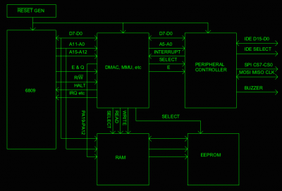
6809v2schema.png [ 42.07 KiB | Viewed 2296 times ]


Though this is a 6809 computer, I think probably 95-99% of the design is in fact generic.

Hopefully you can make some sense of the diagram, though I admit that diagraming is not one of my strong points. Of course very little of this is implemented so far, nor have devices been properly chosen etc. Peripheral ICs (VIAs etc) are fairly obvious extensions of the memory devices, but with their own chip selects and interrupt lines.

PLD 1, the DMAC, MMU and core logic:

:arrow: DMAC which will operate as a cycle stealer though HALT cycles. Arbitary addressing on the source and destination, as well as a (probably limited to 64KByte) length field. Will operate on physical addresses (I think). Optional increments on both source and destination. Interrupt generator when transfer is complete.
:arrow: MMU. I think I described this quite completely in a previously post, so wont repeat it here.
:arrow: Address decoding of the physical addresses. Memory map described later in this post.
:arrow: READ and WRITE gated from E (clock) and R/W
:arrow: Interrupt routing, for NMI, FIRQ, IRQ, with mask registers for all three, as well as a current status register (hopefully I won't need more then 8 interrupts)
:arrow: RESET generation from /RESET (this is needed by the DUART)
:arrow: Random glue logic for the AY sound IC, and VDC

PLD 2, the "peripheral controller":

:arrow: Primitive IDE interface, such that a 16bit IDE device appears transparently as an 8 bit device (such that the DMA controller can pull of a disk block) - some details, like which lines need to be directly attached to the IDE port and which can come from the MPU bus, are a bit fuzzy
:arrow: SPI interface - something like the awesome 65SPI (hopefully I can find the similar VHDL version and get it working)
:arrow: Simple sounder interface

So the memory map. Fairly simple really. Physical address is 20 bits. Must admit I've not thought this through completely yet. :)

Code:
0x00000 - 0x7ffff : 512 KB RAM
0x80000 - 0x9ffff : DMAC/MMU registers
0xa0000 - 0xa002f : IDE/SPI/buzzer registers
0xf0000 - 0xf7fff : 32KB EEPROM


The MMU of course makes the physical address decoding fairly arbitrary, really. There will be one fixed page, at virtual address 0xf000 which will always map to 0xff000 so that the interrupt vectors are always available.

Pin requirements so far look like this:

PLD 1:

12 - address within page
4 - high virtual address
8 - high physical address
8 - databus
2 - clocks (may need only 1, if I don't find a use for Q)
1 - R/W
2 - READ and WRITE
2 - RESET and /RESET
3 - interrupt outputs
1 - halt output
2 - RAM and ROM chip selects

This makes about 45 pins, leaving around 15 for device selects and interrupt inputs. This should be just enough, though of course I can do decoding in another IC if necessary (but I really do not want to)

PLD 2:

1 - chip select
6 - address lines for registers
8 - databus
1 - clock
2 - READ and WRITE
1 - /RESET
1 - interrupt
16 - IDE databus
1 - IDE chip select
8 - SPI selects
3 - SPI MOSI, MISO, CLK
1 - buzzer output line

This makes about 50 lines, leaving some spare.

So the next choice is what PLDs to use. I think the MMU design will demand some fairly heavy logic, and RAM bits to hold the 16 by 8 page table. Probably the neatest thing to do is to use two EPF10K10 in PLCC84, hopefully with both of them programmed from a single EPC2.

If anyone has any suggestions for improvements, criticisms, etc of this very rough idea I would dearly love to hear about it. :)

_________________
8 bit fun and games: https://www.aslak.net/


Top
 Profile  
Reply with quote  
PostPosted: Mon Feb 23, 2015 9:45 pm 
Offline

Joined: Mon Nov 11, 2002 6:53 pm
Posts: 79
Location: Seattle
BigDumbDinosaur wrote:
yzoer wrote:
The one thing I like about CPLD's is the fact that they don't have to be configured on boot. One thing to note though is that 'most' CPLD's only have a re-write span of 100 times or so.

I took a quick look at Atmel's ATF1508AS data sheet and noted that the part is good for 10,000 erase/program cycles.


Yeah, most of those are fine. The EPM7xxx and even the MAX-II are only around 100 times or so. That's why I mentioned it as you'd expect it to be 10k cycles or more!

-Yvo


Top
 Profile  
Reply with quote  
PostPosted: Mon Feb 23, 2015 10:55 pm 
Offline

Joined: Mon Nov 11, 2002 6:53 pm
Posts: 79
Location: Seattle
Aslak3 wrote:
Ok, you have got my interest. :) Are you willing/able to share any of this design? It sounds very impressive, for such a "limited" part. I'm assuming the Xilinx and Altera macrocells are comparable. Do you use VHDL, Verilog, Abel, or something else?


[disclaimer: All of this is from memory!] :-)

I mainly (okay, only) use verilog. For the VGA controller, I run a 25mhz master clock which means you need two 10-bit counters to get the correct timing for a 640x480 standard display (800 pixels across, 525 down). That's about 20 LE's + some additional logic but let's call it 32LE for arguments sake to include for sync generation and what not, which is pretty generous.

The actual display is scan-doubled both horizontally and vertically, which means that the resolution is really 320x240. However, I like my power-of-two's, so I cut down the actual visible portion to 256x192 (really 512x384). A nice benefit of that is that you get more blanking time :-) Another cool counter trick I picked up from old arcade games is that rather than going from 0..511 and then doing a compare to reach 799, you can go from 1024-800=224..1023, which puts the blanking period BEFORE your active scan and moves the active portion from 512-1023, which means you know you're in active scan or blanking when bit 9 is set. It also allows you to use the carry to enable the vertical counter. Same trick again there. Both carry-outs are used to reload their respective counters. In order to use this scheme though, you'll have to move your h- and vsync signals accordingly.

During active scan, the h/v counters directly index into a 256x256x8 page, or 64k with a page bit determining which page is being addressed, i.e. { page, v[7:0], v[7:0] }. In my case this was a single 128Kx8 static ram at 55ns. Given that I'm running at half the VGA resolution, I divide the master clock down by two to get a 12.5mhz clock (80ns access time) which gives me some wiggle room for multiplexing the bus. From a pinout perspective, it looks something like this:

vram address lines: 17
vram data lines: 8
hvrgb: 8 ( hsync, vsync, r:2, g:2, b:2)
vram_we: 1
vram_oe: 1 (/cs is always fixed)
cpu_rw: 1
cpu_be: 1
cpu_sync: 1
cpu_int: 1
cpu_rom: 1
cpu_ram: 1
cpu data: 8
cpu_address: 16

total #of pins = 65

The screen is direct-color RGB (2 bits for each r, g and b) as the CPLD doesn't have enough memory for a programmable palette. An alternative solution would be to create a fixed lookup table and have a higher resolution video DAC. This would also allow you to pack your source data to say, 4bpp. Anyway, each screen takes 48k and I waste (blasphemy!) about 16k of that to make my life easier by having each buffer be aligned to 64k. So the top address line bit determines the buffer / page. The VRAM front-end is basically a mux between the (h/v) counters for reading the screen displayed and the counters (below) for writing. I restricted writing to VRAM to blanking only to make things easier.
With VGA the same line is scanned twice, which sucks and takes up another 48k of bandwidth. grrrrr

For writing data to VRAM, I use two 8-bit registers for the X/Y (into the current page) destination position and 8-bit 'Tile' number for the source. That's another 24LE, rounding that up to 32 for additional glue and I still have 48LE left for the DMA controller.

The DMA controller register writes a 16x16 sprite (256 byte) rectangle to the screen with transparency (based on a 'chroma key') color (unfortunately another 6 LE). It's really nothing more than the two 4-bit loadable counters (8 more LE's) that get added to the X/Y registers above. The carry from the horizontal 4-bit counter is used as an enable to the vertical 4-BIT counter, whereas the carry from the vertical counter acts as a flag to release the bus. The other nice thing is that by combining the 'Tile' register with the two counters, you create your source address without having separate counters. I.e. in verilog, source = { tile, y, x } whereas the destination address is just the two registers and active page { page, y, x }. So by re-using stuff you already have, the DMA engine is pretty much stateless in that you enable the x-counter once you write the tile register while the counters take care of creating both source and destination, no extra registers required. The downside is that your tiles / images will need to be aligned to 256 bytes.

Because the CPU and vram buses are separate, you're effectively reading/writing at the same time.

The only 'real' state-machine is the logic for acquiring the CPU bus and making sure that everything gets scheduled at the right time. A lot of signal re-use here can be used as well as you have a ton of information. The master clock can be divided down again for a 6.25mhz clock (160ns for the CPU).

Last but not least, the scanout performs a clear every other pixel on the odd line of the scan-doubled line, auto-clearing VRAM. Most of this is from memory but now that I've started talking about it again I'll see if I can dig it up :-)

There are still a number of improvements that can be made, such as releasing the bus during active scan if you're not done and triggering an (additional) interrupt when the transfer is complete. Right now the only interrupt is generated once every vblank and the CPU is blocked during this case. Faster VRAM (i.e. CY7c199) allows you for more flexibility and scheduling reads / writes inbetween pixel reads.

Some other cool tricks you can do is to have horizontal / vertical flipping by propagating a hflip/vflip bit and XOR'ing this with the 4-bit counters, which means you have to store far less data.


-Yvo


Top
 Profile  
Reply with quote  
PostPosted: Mon Jun 08, 2015 7:01 pm 
Offline

Joined: Mon Aug 05, 2013 10:43 pm
Posts: 258
Location: Southampton, UK
After a long delay, and some frustrating experiences I have finally made some progress worth reporting. In the end I've gone for the EPF10K10 in PLCC84. I have yet to make up a board for the computer but I have at least got nearly all the parts and knowledge I should need to do so.

Some might be appalled, some surprised but I have made myself a development/experiment system out of this FPGA attached to... solderless breadboard. It actually works quite well and is surprisingly reliable. A EPC2 flash holds the design, though the FPGA can also be programmed directly. Here's a pic of the "dev board" with 16 bit up down counter, hex displayed on some seven segments:

Attachment:
IMAG1365.jpg
IMAG1365.jpg [ 279.89 KiB | Viewed 2221 times ]

I'm still amazed it works so well. Some hookups are 20cm long. You can also see an adapter board I made up for the 84 pin PLCC.

The next step is to join this contraption up to my SBC and see if I can get the two talking to each other! Then I will start on writing the VHDL for the MMU etc.

One question. Well perhaps two. The DMAC uses a HALTing bus stealing method. I'm concerned that during startup whilst the flash is programming the FPGA the /HALT line on the CPU will be tristate, which you should never do. Is a pull-up resistor a simple way to solve this, or should I be doing something more complex? I've also got to deal with /RESET on the CPU. Currently I'm using a reset generator, but there is the possibility that the FPGA will still be being programmed when the reset generator releases /RESET.

_________________
8 bit fun and games: https://www.aslak.net/


Top
 Profile  
Reply with quote  
PostPosted: Fri Jan 08, 2016 12:10 pm 
Offline

Joined: Mon Aug 05, 2013 10:43 pm
Posts: 258
Location: Southampton, UK
After about ten months of research, planning, lots of prototyping, switching CAD tools, then finally drawing up the schematic and laying out the board, I at last have a system I can implement, amongst other things, a DMAC on.

As I've said, I'm using a 6809 as my CPU. For the context of the programmable logic, I suspect this changes nothing. The DMAC is the bus mastering whilst the CPU halts variety. About a month or so ago, after I'd done pretty much all of the design I learned how DMACs can be used to tie a peripheral to memory, using extra peripheral pins which tell the peripheral to drive the databus whilst memory is configured to write, or vica-versa. This sounds cool, and its a shame I didn't learn about it earlier. Nonetheless I'm very pleased with what I've come up with so far.

The FPGAs I settled on, the EPF10K10 in PLCC84 have worked out very well. One forms the core logic: address decoding and other minuitia, and is wired in so it can master the busses for the DMAC. It also generate 8 bits of address at the top of the physical/memory address bus so it can eventually implement a simple MMU/memory mapper I intend to design. Currently the computer only uses the CPUs memory space.

The other FPGA is mostly peripheral and will eventually include a SPI controller, IDE "latch", as well as driving a buzzer and LED, the latter of which was very useful in the bring up. The second FPGA also routes interrupt lines but unfortunately due to an oversight can't present the vector to the databus :( I could do the next best thing though and add registers which are loaded with ISR addresses for each device, just to speed up interrupt processing.

So far, as in I got the basic controller working only yesterday, the following registers are available on the DMAC:

:arrow:16 bit source, destination and length fields
:arrow: 8 bit flags

Flag bits configure wether to increment source and destination. It's also possible, for fun, to negate the source before copying. Finally it is possible to use the controller to memory fill, and thanks to the negation feature you can fill with 0s or 1s. Speed is 1 tick a byte filling, 2 ticks a byte for copying. I have mostly been testing by doing EEPROM to RAM copies so far.

Resource utilisation is looking good so far, and should give me enough room to add a few more features to the DMAC and tackle the MMU. I have yet to look at utilising the RAM bits in these FPGAs. Presumably it will reduce logic resource usage if I can move the registers from logic to these RAM bits.

I still want to look at making "rate limited" transfers possible. If I ever get that multitasking operating system written it will be useful to stagger transfers so the CPU can still have some time. I'm sure there are other things that would be useful.

Even though these FPGAs are 15 years old and no longer made, they are amazing little devices and I think make nice companions to our CPUs. They are not impossible to get hold of, but obviously are not current parts. Of course the obvious question is: Why not just use an FPGA for the whole computer? Well, that wouldn't be as much fun, but I'm sure I will go that route some day, but it will be with my own CPU design.

I must admit I am not taking a very rigerous approach. I'm still very much learning the tools and VHDL. I really want to prove the design via simulation, but have yet to learn how. An element of trial and error has certainly been deployed.

If anyone is interested in the hardware here is the board. The picture is a bit of out date; I've since soldered up the OPL2/YM3812, which works well.

Attachment:
IMAG0059.jpg
IMAG0059.jpg [ 40.39 KiB | Viewed 2147 times ]


Yeap it's big. Have yet to finish the assembly but couldn't wait to get started with the programmable logic. :)

There's more about the bring up, what other features the micro has, etc etc in my blog.

_________________
8 bit fun and games: https://www.aslak.net/


Top
 Profile  
Reply with quote  
PostPosted: Fri Jan 08, 2016 3:33 pm 
Offline
User avatar

Joined: Fri Dec 11, 2009 3:50 pm
Posts: 3363
Location: Ontario, Canada
Nice work, Aslak3 -- congratulations on your success! Since you have now graduated this project from a breadboard implementation to a mature design, it strikes me that a new thread may be justified in order to introduce MAXI09 properly. I'd be interested to see a block diagram, and/or a summary of the peripherals and other features. A larger photo would be nice, too. :)

Aslak3 wrote:
after I'd done pretty much all of the design I learned how DMACs can be used to tie a peripheral to memory [...] Nonetheless I'm very pleased with what I've come up with so far.
If I understand properly, your DMA scheme uses two bus cycles for each byte transferred. One of these cycles activates the peripheral device -- its address is placed on the address bus, causing the device to respond, and the byte is buffered briefly in the DMAC on its way to/from memory. (The alternative scheme you mentioned uses one bus cycle per byte transferred. Only the memory address appears, and extra logic is required to coax the peripheral to respond. The byte is transferred directly, not buffered.)

Aslak3 wrote:
a simple MMU/memory mapper I intend to design [...] Why not just use an FPGA for the whole computer? Well, that wouldn't be as much fun, but I'm sure I will go that route some day, but it will be with my own CPU design.
If you want a gratifying challenge, how about keeping your 6809 but "expanding" the 6809 instruction set to include instructions that talk directly to your memory mapper? I put the word expanding in quotation marks because really all you need is to identify some unused corners of the existing 6809 instruction set, and create hardware to watch for those. The 6809 needn't learn any new tricks, only the external hardware. Having expanded the 65c02 instruction set to include memory mapping, I can assure you this sort of thing is both possible and fun! If you're gonna be designing a memory mapper anyway...

cheers,
Jeff

_________________
In 1988 my 65C02 got six new registers and 44 new full-speed instructions!
https://laughtonelectronics.com/Arcana/ ... mmary.html


Top
 Profile  
Reply with quote  
PostPosted: Fri Jan 08, 2016 5:29 pm 
Offline

Joined: Mon Aug 05, 2013 10:43 pm
Posts: 258
Location: Southampton, UK
Dr Jefyll wrote:
Nice work, Aslak3 -- congratulations on your success! Since you have now graduated this project from a breadboard implementation to a mature design, it strikes me that a new thread may be justified in order to introduce MAXI09 properly. I'd be interested to see a block diagram, and/or a summary of the peripherals and other features. A larger photo would be nice, too. :)


Thanks. :) I could do, but I was a bit reluctant since I don't use a 65xx in my design (except a 6522, hehe). Otherwise I'd love to tell everyone all about it! If it is ok, what forum should I use? Hardware?

Aslak3 wrote:
If I understand properly, your DMA scheme uses two bus cycles for each byte transferred. One of these cycles activates the peripheral device -- its address is placed on the address bus, causing the device to respond, and the byte is buffered briefly in the DMAC on its way to/from memory.


Yes exactly. It's nice because no special support is needed from the peripheral. You can do memory to memory copies etc. I'm only a tiny bit frustrated that I can't implement the "direct" approach from a gaining knowledge point of view. But it would still have been interesting to use it on my QUART, which has pins for these kinds of transfers. Oh well. 2 clock ticks to copy a byte is still a lot faster then the CPU could do it. :)

Quote:
If you want a gratifying challenge, how about keeping your 6809 but "expanding" the 6809 instruction set to include instructions that talk directly to your memory mapper? I put the word expanding in quotation marks because really all you need is to identify some unused corners of the existing 6809 instruction set, and create hardware to watch for those. The 6809 needn't learn any new tricks, only the external hardware...


Hmm! That sounds extremely interesting, but I'm not sure I can implement such a mechanism, since the FPGA does not sit between the CPU and memory on the databus? Therefore it can't modify the opcode stream to replace the new command with NOPs or whatever. Whilst the FPGA could peek at the data the memory is presenting, the CPU would surely crash if it got unknown opcodes?

Otherwise that sounds intriguing! Unless I'm missing something?

Thanks for the feedback.:) MAXI09 is certainly going to keep me busy, probably for the whole year!

_________________
8 bit fun and games: https://www.aslak.net/


Top
 Profile  
Reply with quote  
PostPosted: Fri Jan 08, 2016 6:32 pm 
Offline
User avatar

Joined: Fri Dec 11, 2009 3:50 pm
Posts: 3363
Location: Ontario, Canada
Dr Jefyll wrote:
If I understand properly, your DMA scheme uses two bus cycles for each byte transferred. One of these cycles activates the peripheral device -- its address is placed on the address bus, causing the device to respond, and the byte is buffered briefly in the DMAC on its way to/from memory.
Aslak3 wrote:
Yes exactly. It's nice because no special support is needed from the peripheral. You can do memory to memory copies etc. I'm only a tiny bit frustrated that I can't implement the "direct" approach from a gaining knowledge point of view. But it would still have been interesting to use it on my QUART, which has pins for these kinds of transfers. Oh well. 2 clock ticks to copy a byte is still a lot faster then the CPU could do it. :)
Yes indeed, still a lot faster than the CPU could do it. And the even-faster approach is tough to implement unless the peripheral does have pins for these kinds of transfers.

Dr Jefyll wrote:
it strikes me that a new thread may be justified in order to introduce MAXI09 properly.
Aslak3 wrote:
Thanks. :) I could do, but I was a bit reluctant since I don't use a 65xx in my design (except a 6522, hehe). Otherwise I'd love to tell everyone all about it! If it is ok, what forum should I use? Hardware?
Oops, I'd forgotten your project will be considered marginally OT by some of our members. I can't speak on their behalf. But I don't think there can be any argument that the DMA aspect of your work isn't squarely relevant. That's because 65xx and 68xx (not to be confused with 68xxx) families both use memory-mapped I/O and have bus interfaces which are virtually identical.

Dr Jefyll wrote:
If you want a gratifying challenge, how about keeping your 6809 but "expanding" the 6809 instruction set to include instructions that talk directly to your memory mapper?
Aslak3 wrote:
Hmm! That sounds extremely interesting, but I'm not sure I can implement such a mechanism, since the FPGA does not sit between the CPU and memory on the databus?

I doubt it would be necessary to intercept and translate opcodes. (My KK computer does that for some of the new instructions, but its goals go beyond memory mapping; for example it includes instructions for Forth and video. Plus, the KK has no FPGA!) So, KK is not a good comparison. Different problems to solve, and different solutions available. One big challenge is managing without the 65xx's SYNC pin (to help parse instructions), but I expect this is surmountable.

IIRC Rob Finch's RTF6809 core expands the instruction set by watching for a relative branch (not taken!) whose offset is $FF. That unique cue acts as a prefix to alter the meaning of the following instruction. And, in your situation, the meaning of the following instruction is easy to alter just by inhibiting memory during a specific cycle (or cycles) and engaging an FPGA register instead. For example, load immediate from one of the memory-map registers. I'm only scratching the surface here -- it's certainly NOT a comprehensive list of the possibilities. (And many of the possibilities map to 65xx, BTW.)

I'd still like to see a proper photo, a block diagram and a summary of the MAXI09 features. :)

ETA: maybe you'd like to create a MAXI09 topic over on the forum at anycpu.org. You'll find some of The Usual Suspects from 6502.org there, and any cpu is safely ON topic. :)

-- Jeff

_________________
In 1988 my 65C02 got six new registers and 44 new full-speed instructions!
https://laughtonelectronics.com/Arcana/ ... mmary.html


Top
 Profile  
Reply with quote  
PostPosted: Fri Jan 08, 2016 8:15 pm 
Offline
User avatar

Joined: Thu May 28, 2009 9:46 pm
Posts: 8198
Location: Midwestern USA
Aslak3 wrote:
Dr Jeffyl wrote:
If I understand properly, your DMA scheme uses two bus cycles for each byte transferred. One of these cycles activates the peripheral device -- its address is placed on the address bus, causing the device to respond, and the byte is buffered briefly in the DMAC on its way to/from memory.

Yes exactly. It's nice because no special support is needed from the peripheral. You can do memory to memory copies etc. I'm only a tiny bit frustrated that I can't implement the "direct" approach from a gaining knowledge point of view. But it would still have been interesting to use it on my QUART, which has pins for these kinds of transfers. Oh well. 2 clock ticks to copy a byte is still a lot faster then the CPU could do it. :)

Good work!

On a 65C816 system running at 20 Mhz, your DMAC would theoretically be capable of moving 10 MB/second. To put that into perspective, the 65C816's MVx copy functions process at the rate of one byte per seven clock cycles, hence can manage a maximum of 2.86MB/second, neglecting time consumed by interrupt processing. Ergo your DMAC when used as a "blitter" would be about 3.5 times faster. That's certainly not shabby.

Incidentally, if I had a DMAC with that level of performance as part of POC I'd be able to run the SCSI bus in fast synchronous mode, which happens to be a 10 MB/second transfer rate. In practical terms, that level of performance would pop 64KB of data from disk to core in about 6.5 milliseconds. I could live with that. :D

Of course, the "holy grail" would be to get the DMAC to put the source device in read mode, the destination device in write mode and have the transfer occur on the rise of the clock. The resulting 20 MB/second performance would allow me to run the SCSI bus in FAST-20 synchronous mode, theoretically cutting that 6.5 ms data load to 3.25 ms. I could live with that as well! :lol:

_________________
x86?  We ain't got no x86.  We don't NEED no stinking x86!


Top
 Profile  
Reply with quote  
PostPosted: Sun Jan 10, 2016 6:25 pm 
Offline
User avatar

Joined: Fri Dec 11, 2009 3:50 pm
Posts: 3363
Location: Ontario, Canada
Dr Jefyll wrote:
how about keeping your 6809 but "expanding" the 6809 instruction set to include instructions that talk directly to your memory mapper?
Aslak3 wrote:
I'm not sure I can implement such a mechanism, since the FPGA does not sit between the CPU and memory on the databus? Therefore it can't modify the opcode stream to replace the new command with NOPs or whatever.
I'll return to this to clarify. The new instruction needn't take the form of an illegal aka undefined opcode (which would muck up the works if not replaced with a NOP). A relative branch (never taken) with offset $FF is just one example of a benign but quirky encoding that's virtually never encountered and thus can have new meaning attached to it. You could also use ORA # 0 or AND #$FF, and have the FPGA recognize that -- either as a simple self-contained instruction, or as a prefix that causes the memory mapper to co-execute the subsequent instruction. Finding other quirky unused encodings requires only imagination. For example on 6809 you could use multiple prefix bytes (all but one are ignored), or LEAX 0,X (basically NOP). I'm sure there are others.

Illegal opcodes do offer more potential, though. And, luckily, replacing them with NOPs doesn't require the FPGA to sit between the CPU and memory (although that option is viable). Even if the CPU, memory & FPGA all tie to a single data bus, a new opcode can be recognized by the FPGA near the end of the bus cycle which fetched it. The FPGA deasserts RDY, or stretches the clock, so the CPU won't eat the bad opcode. During the resulting extra time, the FPGA inhibits memory so the data bus is tristated, then places the NOP or whatever on the bus for consumption by the CPU. (Some members of the 65xx family have undefined instructions which, conveniently, already are NOP's. The 'C02 has 32 single-byte NOP's plus some multi-byte versions, and the 816's 2-byte WDM instruction has 256 possible encodings, all NOP.)

BigDumbDinosaur wrote:
[regarding DMA] Of course, the "holy grail" would be [...] 20 MB/second performance
Interestingly, this is probably achievable without a DMA controller. I believe Don Lancaster's "cheap video" technique can be adapted to the task. Thanks to cheap video, the 5 MHz Rockwell CPU in my KK Computer can output up to 5 MB/second -- IOW a transfer rate of one clock per byte. Running a WDC CPU at 20 MHz one could input or output 20 MB/second from a disk controller. (6809's can use the cheap video technique, too! Even the Z80-based Timex Sinclair ZX81 uses a form of cheap video.)

_________________
In 1988 my 65C02 got six new registers and 44 new full-speed instructions!
https://laughtonelectronics.com/Arcana/ ... mmary.html


Top
 Profile  
Reply with quote  
Display posts from previous:  Sort by  
Post new topic Reply to topic  [ 27 posts ]  Go to page Previous  1, 2

All times are UTC


Who is online

Users browsing this forum: No registered users and 17 guests


You cannot post new topics in this forum
You cannot reply to topics in this forum
You cannot edit your posts in this forum
You cannot delete your posts in this forum
You cannot post attachments in this forum

Search for:
Jump to:  
cron